
Two-dimensional vertical cavity surface emitting laser array

A vertical-cavity surface-emitting laser technology, applied in the field of laser arrays, can solve problems such as limiting high-density integration applications

Active Publication Date: 2014-04-16
HI TECH OPTOELECTRONICS
View PDF5 Cites 11 Cited by
  • Summary
  • Abstract
  • Description
  • Claims
  • Application Information

AI Technical Summary

Problems solved by technology

However, for the vertical cavity surface emitting laser array arranged in a square shape, the size of the entire array will also increase with the increase of the cell pitch, which limits its application in high-density integration.

Method used


Image

  • Two-dimensional vertical cavity surface emitting laser array
  • Two-dimensional vertical cavity surface emitting laser array
  • Two-dimensional vertical cavity surface emitting laser array

Examples


Embodiment Construction

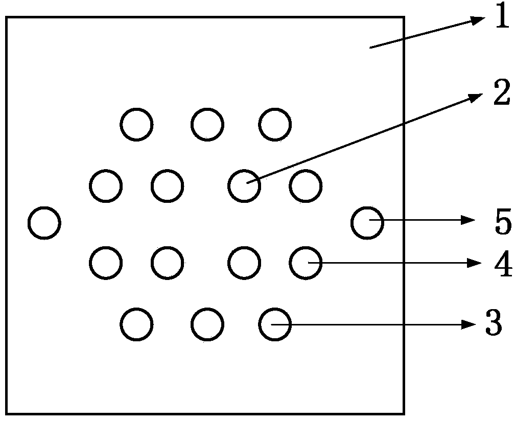
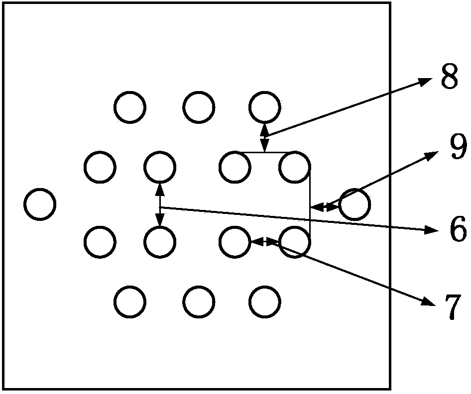
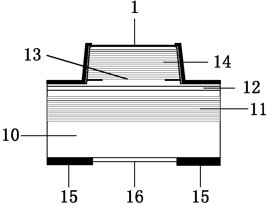
[0018] Such as Figure 1-3 As shown, this two-dimensional vertical cavity surface-emitting laser array includes a surface electrode 1 and n unit laser devices, n is an integer greater than 3, and the unit laser devices are distributed on the surface electrodes, and the unit laser devices include (n -2) 2 2 central unit laser devices, (n-1)*2 horizontal peripheral unit laser devices 3, (n-2)*2 vertical peripheral unit laser devices 4, 2 edge unit laser devices 5, each unit laser The diameter of the active area of ​​the component is d and the light exit aperture is r, the distance 6 between two adjacent central area unit laser devices is D, D>d, the vertical peripheral unit laser device and the adjacent central area unit laser device are in the On the same horizontal line and the distance 7 between the two is d, the horizontal peripheral unit laser device is located on the mid-perpendicular line of two adjacent central area unit laser devices and the distance 8 from the mid-sag...


PUM


Abstract

The invention discloses a two-dimensional vertical cavity surface emitting laser array. The two-dimensional vertical cavity surface emitting laser array comprises a surface electrode and n unit laser devices, wherein n is an integer which is larger than 3; the unit laser devices are distributed on the surface electrode; the unit laser devices comprise (n-2) <2> central area unit laser devices, (n-1) * 2 horizontal peripheral unit laser devices, (n-2) * 2 vertical peripheral unit laser devices and two edge unit laser devices; the active area diameter of every unit laser device is d and the light aperture of every unit laser device is r. According to the two-dimensional vertical cavity surface emitting laser array, the arrangement mode which is similar to a rhombus is adopted and accordingly the thermal crosstalk is low and the unit density is large in the same surface electrode area, the temperatures of the unit laser devices are uniformly distributed at different coupling positions, the integral temperature of the array is low, the thermal effect of a high power vertical cavity surface emitting laser array is significantly improved, the output performance of the devices is improved, and the application fields of lasers are extended.

Description

technical field [0001] The invention belongs to the technical field of semiconductor laser devices, in particular to a two-dimensional vertical cavity surface emitting laser array. Background technique [0002] Due to its low threshold current, low output beam divergence angle, and low cost, vertical cavity surface emitting lasers have attracted widespread attention in high-speed data transmission, high-resolution printing, and pumping solid-state lasers and fiber lasers. In recent years, with the continuous expansion of the application field of vertical cavity surface emitting lasers, higher requirements have been put forward for its output power. [0003] Integrating each single tube unit into a two-dimensional array on a single chip is one of the effective methods to increase the output power of the vertical cavity surface emitting laser. Higher integration and proper heat dissipation can make this two-dimensional array easier Get high power output. However, due to the ...

Claims


Application Information

Patent Timeline
Patent Type & Authority Applications(China)
IPC IPC(8): H01S5/42
Inventor 刘迪王晓薇
Owner HI TECH OPTOELECTRONICS
Learn More