
Printed circuit board with barrier dam protection layer

A printed circuit board and protective layer technology, applied in the direction of printed circuits connected with non-printed electrical components, can solve the problems of not being covered by green oil, drift, etc., and achieve high use value, stable performance, and no device drift. Effect

Inactive Publication Date: 2014-04-09
SHANGHAI RAILWAY COMM
View PDF5 Cites 0 Cited by
  • Summary
  • Abstract
  • Description
  • Claims
  • Application Information

AI Technical Summary

Problems solved by technology

However, for the power amplifier board produced by our company, due to its heat dissipation, a large area of ​​copper foil needs to be exposed and cannot be covered by green oil.
This causes the printed board to be unable to stay in the required position after tinning, and the solder paste will expand along the copper foil, which will cause the components to be soldered on the solder paste to drift with the expansion of the solder paste

Method used


Image

  • Printed circuit board with barrier dam protection layer
  • Printed circuit board with barrier dam protection layer

Examples


Embodiment 1

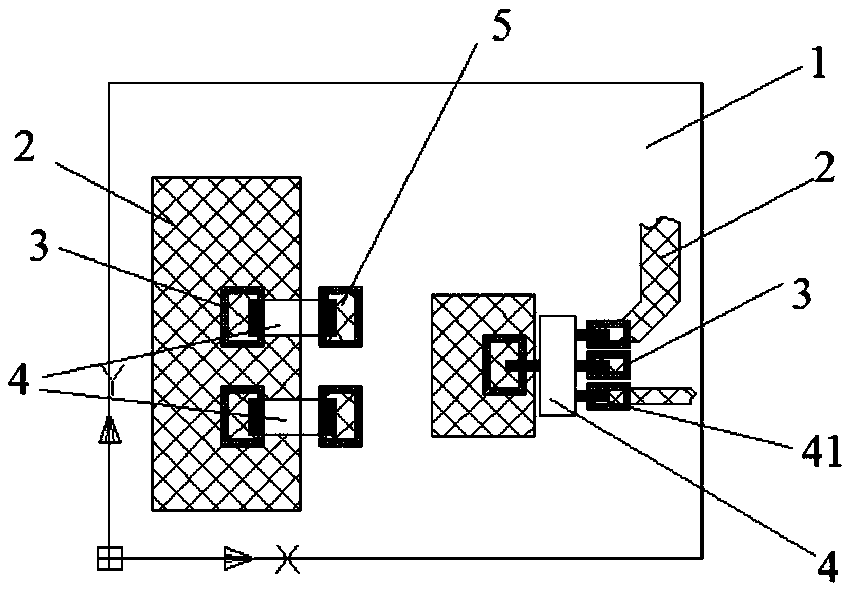
[0018] Such as figure 1 and 2 As shown, a printed circuit board with a dam protection layer includes a substrate 1, a circuit copper foil 2, a pad 5, a dam 3 and a device 4, and the circuit copper foil 2 is fixed on the substrate 1, and the The pad 5 and the dam 3 are respectively fixed on the line copper foil 2, the device 4 is welded on the pad 5 by soldering the device pin 41, the pad 5 is surrounded by the dam 3, and the Solder 6 packs inside.

[0019] The dam is a rectangular frame with the same area as the pad and a frame width of 0.2. Described dam is green oil dam or silk screen printing ink dam.

[0020] The process flow of the printed circuit board of the present invention is: single-sided copper clad board-cutting-photochemical method / screen printing image transfer-removal of anti-corrosion printing material-cleaning-drying-hole processing-shape processing-cleaning and drying - Curing - Rinsing and Drying - Pre-Fluxed - Drying - Finished Product.

[0021] The C...

Embodiment 2

[0023] The frame width is 0.5mm. Others are the same as embodiment 1.

Embodiment 3

[0025] The frame width is 1.0mm. Others are the same as embodiment 1.


PUM


Abstract

The invention relates to a printed circuit board with a barrier dam protection layer. The printed circuit board comprises a substrate, circuit copper foil, bonding pads, barrier dams and devices. The circuit copper foil is fixed to the substrate, the bonding pads and the barrier dams are respectively fixed to the circuit copper foil, the devices are welded to the bonding pads through soldering tin, the barrier dams surround the bonding pads, and the soldering tin is wrapped inside. Compared with the prior art, the printed circuit board has the advantages that when the printed circuit board is printed, solder paste cannot be extended, the devices cannot shift, and meanwhile meanwhile the design requirement for large-area copper foil heat radiation can be met.

Description

technical field [0001] The invention relates to a printed circuit board, in particular to a printed circuit board with a dam protection layer. Background technique [0002] The current printed circuit boards will see green coverage on the surface, which is green oil. This is a protective layer that is applied to the traces and substrate of the circuit board that do not require soldering. The purpose is to prevent the flow of solder and act as a solder mask. However, for the power amplifier board produced by our company, due to its heat dissipation, a large area of ​​copper foil needs to be exposed and cannot be covered by green oil. This causes the printed board to be unable to stay in the required position after tinning, and the solder paste will spread along the copper foil, causing the components to be soldered on the solder paste to drift with the expansion of the solder paste. Contents of the invention [0003] The purpose of the present invention is to provide a p...

Claims


Application Information

Patent Timeline
Patent Type & Authority Applications(China)
IPC IPC(8): H05K1/18
Inventor 侯晶吴波李毅力唐莹马康曹剑锋余园园王志孝陈小英
Owner SHANGHAI RAILWAY COMM
Learn More