Method for reverse diffusion

A diffusion method and reverse diffusion technology, applied in the field of reverse diffusion, can solve the problems of increasing the diffusion process time, affecting the uniformity of the square resistance, and the controllability of the uniformity of the square resistance becoming worse.

Active Publication Date: 2014-04-09
CHINT NEW ENERGY TECH (HAINING) CO LTD
View PDF5 Cites 2 Cited by
  • Summary
  • Abstract
  • Description
  • Claims
  • Application Information

AI Technical Summary

Problems solved by technology

[0004] To reduce the surface doping concentration, the most commonly used method is to reduce the flux of the phosphorus source, but this method will make the phosphorus source not fully mixed in the diffusion gas, which will cause uneven internal resistance of the silicon wafer after diffusion; at the same time, due to the phosphorus The source content is small, so to a large extent, the concentration of the phosphorus source at the inlet and outlet of the diffusion furnace has a large difference in phosphorus source concentration. This concentration difference will cause a large difference in the square resistance between the diffusion silicon wafers, that is The uniformity of square resistance becomes worse
In addition, due to the low concentration of phosphorus source, it is necessary to increase the diffusion process time or increase the diffusion temperature under the premise of ensuring sufficient doping amount; and in the case of low phosphorus source, high temperature diffusion will further affect the square resistance. Uniformity
[0005] To sum up, although reducing the phosphorus source concentration can reduce the impurity concentration on the surface of the silicon wafer to a certain extent, it will correspondingly increase the process time or make the controllability of the square resistance uniformity worse. A Diffusion Method That Can Realize Low Doping Concentration on Silicon Wafer Surface Without Reducing Phosphorus Source Concentration

Method used


Image

  • Method for reverse diffusion
  • Method for reverse diffusion
  • Method for reverse diffusion

Examples


Embodiment Construction

[0026] The following disclosure provides many different embodiments or examples for implementing different structures of the present invention. To simplify the disclosure of the present invention, components and arrangements of specific examples are described below. Furthermore, the present invention may repeat reference numerals and / or letters in different instances. This repetition is for the purpose of simplicity and clarity and does not in itself indicate a relationship between the various embodiments and / or arrangements discussed. It should be noted that components illustrated in the figures are not necessarily drawn to scale. Descriptions of well-known components and processing techniques and processes are omitted herein to avoid unnecessarily limiting the present invention.

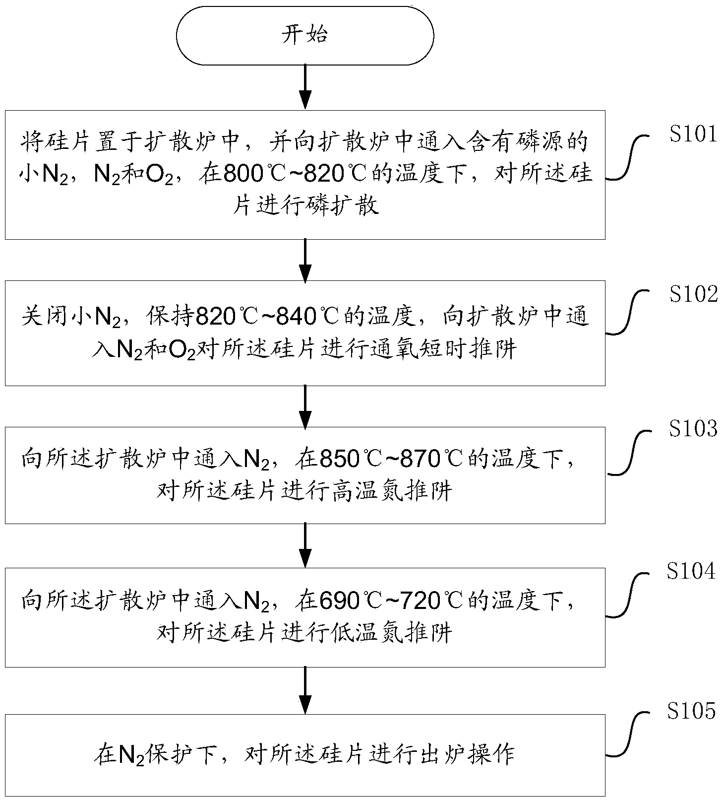
[0027] refer to figure 1 , figure 1 Shown is a schematic flow chart of a specific embodiment of a method for reverse diffusion provided by the present invention.

[0028] Step S101, placing th...


PUM


Abstract

The invention discloses a method for reverse diffusion. The method comprises the following steps: placing a silicon wafer to a diffusion furnace, inletting small N2 containing a phosphorus source, N2 and O2 to the diffusion furnace, and carrying out phosphorus diffusion on the silicon wafer under the temperature ranging from 800 DEC to 820 DEC; closing the small N2, keeping the temperature to be 820-840 DEC, inletting N2 and O2 to the diffusion furnace, and carrying out oxygen-inletting short-time drive-in on the silicon wafer; inletting N2 to the diffusion furnace and carrying out high-temperature nitrogen drive-in on the silicon wafer under the temperature of 850-870 DEC; inletting N2 to the diffusion furnace and carrying out reverse diffusion on the silicon wafer under the temperature of 690-720 DEC; and under the protection of the N2, taking the silicon wafer out of the furnace. With the diffusion method provided in the invention, and under the condition of the same doping amount, phosphorus atoms are allowed to have relatively-low doping density on the surface of the silicon wafer, thereby reducing surface recombination and improving an open-circuit voltage and photoelectric conversion efficiency of a solar cell.

Description

technical field [0001] The invention belongs to the technical field of solar cells, and in particular relates to a reverse diffusion method. Background technique [0002] In the solar cell manufacturing process, the manufacture of P-N junction has always been the focus of research. The P-N junction is the core part of the solar cell, and its quality is directly related to the photoelectric conversion efficiency of the solar cell. P-N junctions can be manufactured by various methods such as ion implantation, and diffusion junction is currently the most widely used, so it is also a research hotspot. The quality of the diffusion junction process directly affects the quality of the P-N junction. [0003] The diffusion process determines the distribution of impurities. When the impurity concentration on the surface of the silicon wafer is too high, a diffusion "dead layer" (that is, containing a large number of interstitial atoms and defects) will be formed, so that serious cha...

Claims


Application Information

Patent Timeline
Patent Type & Authority Applications(China)
IPC IPC(8): H01L31/18H01L21/22
CPCH01L21/2225H01L31/1804Y02E10/547Y02P70/50
Inventor 李旺韩玮智牛新伟王仕鹏黄海燕陆川
Owner CHINT NEW ENERGY TECH (HAINING) CO LTD
Why Eureka
Try Eureka