Semiconductor integrated circuit
A technology of integrated circuits, semiconductors, applied in the field of measures against false attacks
- Summary
- Abstract
- Description
- Claims
- Application Information
AI Technical Summary
Problems solved by technology
Method used
Image
Examples
no. 2 example
[0104]
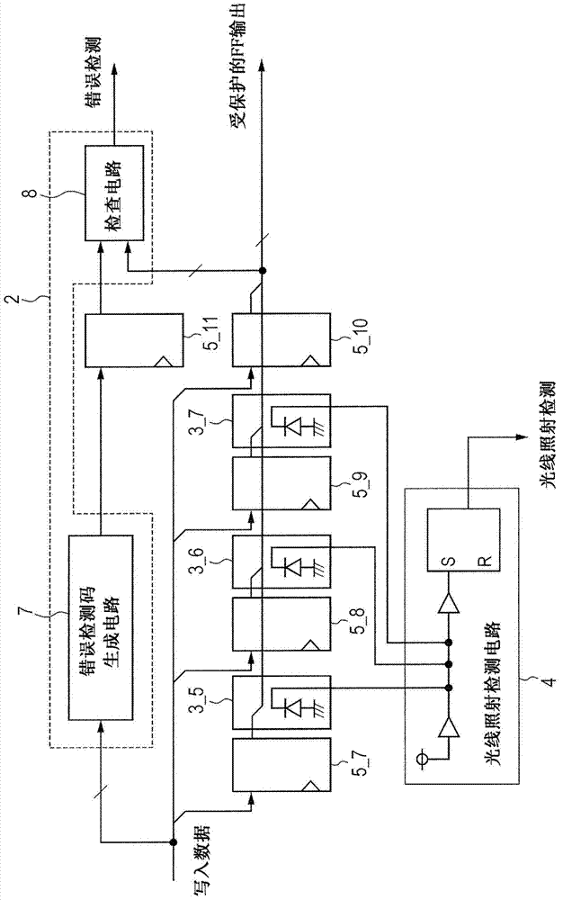
[0105] figure 2 is an explanatory diagram showing a specific configuration example of a semiconductor device according to the second embodiment. In this configuration example, the error determination circuit 2 is capable of detecting a 1-bit error, and the light detection elements 3_5 to 3_7 are interleaved among the storage elements 5_7 to 5_10 so as to detect laser irradiation to 2-bit or more storage elements.
[0106] The semiconductor device includes an error detection code generating circuit 7 for generating an error detection code based on write data stored in flip-flops 5_7 to 5_10. The error detection code generated by the error detection code generation circuit 7 is stored in the flip-flop 5_11. The check circuit 8 determines the presence or absence of an error based on the data read from the flip-flops 5_7 to 5_10 and the error detection code stored in the flip-flop 5_11 , and outputs an error detection signal if there is an error. Outputs of the light...
no. 3 example
[0115]
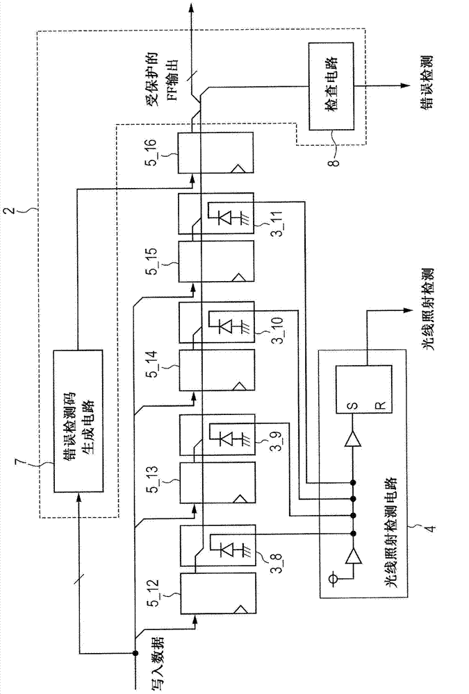
[0116] Although the second embodiment utilizes a 1-bit error detection code, the error detection capability is arbitrarily improved. In the case where the error detection capability of the error determination circuit 2 is improved, the light irradiation detection capability of the light irradiation detection circuit 4 is reduced. In the case where the error determination circuit 2 is capable of detecting errors of m bits or less, it is only necessary for the light irradiation detection circuit 4 to have the ability to detect light irradiation to (m+1) or more storage elements. More specifically, one light detection element is provided for m storage elements.
[0117] Figure 4 is an explanatory diagram showing a configuration example in which a semiconductor device according to a third embodiment adopts a 3-bit error detection code.
[0118] The semiconductor device includes an error detection code generating circuit 7 for generating an error detection code based ...
no. 4 example
[0122]
[0123] Figure 5 is an explanatory diagram showing a configuration example for protection by duplexing of a semiconductor device according to the fourth embodiment.
[0124] Write data is written to the flip-flop 5_24 as the active system and the flip-flop 5_25 as the standby system, and the data stored in the flip-flop 5_24 as the active system is read as a protected FF output. The error detection circuit 2 is an exclusive OR gate, and outputs an error detection signal when the data read from the flip-flop 5_24 and the data read from the flip-flop 5_25 do not match.
[0125] The light detection element 3_14 is arranged between a trigger 5_24 as an active system and a trigger 5_25 as a backup system. Based on its output, the light irradiation detection circuit outputs a light irradiation detection signal.
[0126] An attack is detected as a light detection signal when light is irradiated to one of the flip-flops 5_24 and 5_25 as the active and backup systems to in...
PUM
 Abstract
Description
Claims
Application Information
 - R&D
- Intellectual Property
- Life Sciences
- Materials
- Tech Scout
- Unparalleled Data Quality
- Higher Quality Content
- 60% Fewer Hallucinations
Browse by: Latest US Patents, China's latest patents, Technical Efficacy Thesaurus, Application Domain, Technology Topic, Popular Technical Reports.
© 2025 PatSnap. All rights reserved.Legal|Privacy policy|Modern Slavery Act Transparency Statement|Sitemap|About US| Contact US: help@patsnap.com


