Microwave thin-film capacitor integration method
An integrated method and microwave thin film technology, applied in the direction of thin film/thick film capacitors, laminated capacitors, etc., can solve the problems of large span of the upper electrode, defects in the connection between the upper electrode of the capacitor and the transmission line, and can not meet the design requirements, so as to reduce the production cost. Cost, meeting the requirements of electrical performance indicators, and the effect of production yield
- Summary
- Abstract
- Description
- Claims
- Application Information
AI Technical Summary
Problems solved by technology
Method used
Image
Examples
Embodiment 1
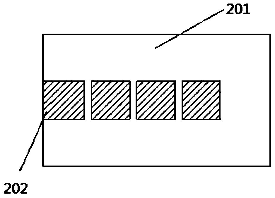
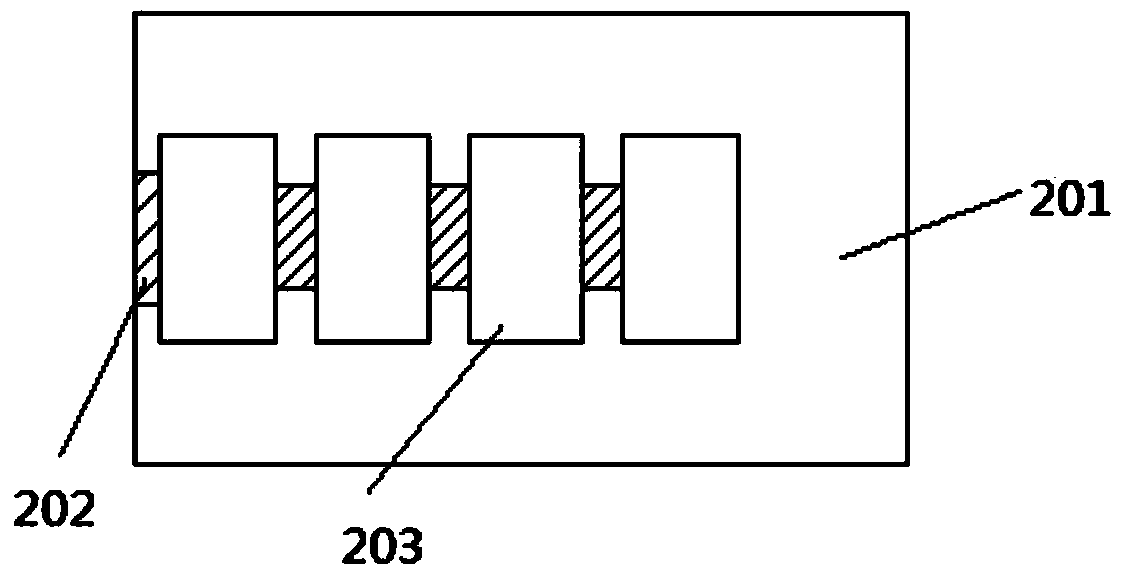
[0029] In this embodiment, a capacitor is decomposed into several capacitors connected in series, so that the consistency of the circuit transmission line width can be maintained, and a capacitance value that meets the requirements can be designed, and the distance between electrodes of each capacitor can be reduced. To reduce the difficulty of process realization, taking 4 capacitors in series as an example, the design scheme and production process are as follows Figure 2-5 As shown, 201 is the substrate among the figure:
[0030] Step 1: Decompose a capacitor into a structure of several capacitors connected in series;
[0031] Step 2: Vacuum coating on the substrate and photoetching the lower electrode pattern such as figure 2 as shown in Section 202 of the
[0032] Step 3: Vacuum coating and photoetching the pattern of the dielectric layer such as image 3 as shown in Section 203 of the
[0033] Step 4: Vacuum coating and photoetching the upper electrode pattern such ...
Embodiment 2
[0038] On the basis of the above embodiment, further, in the first step, the series connection of the capacitors is a series connection of capacitors connected end to end.
[0039] On the basis of the above embodiment, further, in the first step, the number of capacitors is 4 capacitors.
[0040] On the basis of the above embodiments, further, in the first step, the capacitance values of the several capacitors are equal or unequal.
[0041] On the basis of the above embodiments, further, in the third step, the material of the dielectric layer is a dielectric material with a large dielectric constant and a low dissipation factor.
[0042] On the basis of the above embodiments, further, in the third step, the thickness of the dielectric layer is 5000-100000 nm.
[0043] Adopting the above-mentioned scheme solves the difficult problem of making small-capacity thin-film capacitors by using dielectric materials with large dielectric constant and low loss factor, which can greatl...
PUM
 Abstract
Description
Claims
Application Information
 - R&D
- Intellectual Property
- Life Sciences
- Materials
- Tech Scout
- Unparalleled Data Quality
- Higher Quality Content
- 60% Fewer Hallucinations
Browse by: Latest US Patents, China's latest patents, Technical Efficacy Thesaurus, Application Domain, Technology Topic, Popular Technical Reports.
© 2025 PatSnap. All rights reserved.Legal|Privacy policy|Modern Slavery Act Transparency Statement|Sitemap|About US| Contact US: help@patsnap.com


