Chip multilayer ceramic connector and preparation method thereof
A technology of multi-layer ceramics and connectors, which is applied in the direction of connection, fixed connection, contact parts, etc., can solve the problem of large size of circuit connectors, and achieve the effect of small size and miniaturization
- Summary
- Abstract
- Description
- Claims
- Application Information
AI Technical Summary
Problems solved by technology
Method used
Image

Examples
preparation example Construction
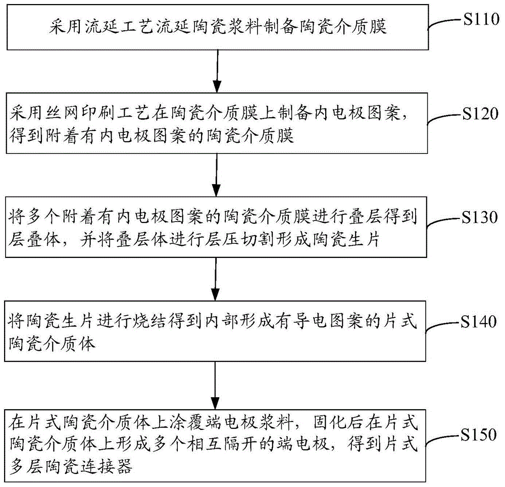
[0051] see image 3 , the preparation method of the chip type multilayer ceramic connector of an embodiment, comprises the following steps:
[0052] Step S110: Casting the ceramic slurry by a casting process to prepare a ceramic dielectric film.
[0053] Ceramic slurry is obtained by mixing porcelain material, organic binder and organic solvent. The ceramic material can be zirconium titanium strontium calcium (Ca-Sr-Ti-Zr) system ceramic material, barium neodymium titanium (Ba-Nd-Ti) system ceramic material or magnesium silicate (MgSiO 3 ) and other system porcelain materials.
[0054] Preferably, the ceramic material contains a general formula of Ca x Sr 1-x (Ti y Zr 1-y ) z o 3 The composite oxide, where 0<x<1, 0<y<1, 0.8<z<1.2.
[0055] Preferably, the ceramic material further includes at least one of Mg oxide, Zn oxide, Si oxide, Mn oxide and Y oxide with a mass fraction of 0.1-5%.
[0056] The above-mentioned ceramic material has high insulation and low electric...
Embodiment 1
[0081] Preparation of multilayer ceramic connectors
[0082] 1. Mix titanium-strontium-calcium (Ca-Sr-Ti-Zr) system ceramic material, organic binder and organic solvent to obtain ceramic slurry, and use a casting process to cast the ceramic slurry to prepare a ceramic dielectric film. Wherein, the organic binder is polyvinyl butyral, and the organic solvent is a mixture of toluene and ethanol at a mass ratio of 1:1. The mass ratio of titanium strontium calcium (Ca-Sr-Ti-Zr) system ceramic material, organic binder and organic solvent is 50:20:30;
[0083] 2. Using a screen printing process to prepare internal electrode patterns on the ceramic dielectric film to obtain a ceramic dielectric film with internal electrode patterns attached. Among them, the diameter of the screen wire is 15 μm, the mesh number of the screen is 500 mesh, the torque of the screen stretcher is 22N / mm, and the exposure time is 20 seconds; the printing speed of the screen printing machine is 100mm / s, and...
Embodiment 2
[0089] 1. It will contain the general formula Ca x Sr 1-x (Ti y Zr 1-y ) z o 3 (0x Sr 1-x (Ti y Zr 1-y ) z o 3 (0<x<1, 0<y<1, 0.8<z<1.2) The mass percentage of the composite oxide is 95%, and the porcelain material also contains 5% magnesium oxide by mass;
[0090]2. Using a screen printing process to prepare internal electrode patterns on the ceramic dielectric film to obtain a ceramic dielectric film with internal electrode patterns attached. Among them, the diameter of the screen wire is 16 μm, the mesh number of the screen is 500 mesh, the torque of the screen stretcher is 25N / mm, and the exposure time is 35 seconds; the printing speed of the screen printing machine is 200mm / s, and the laying speed is 150mm / s, the angle of the scraper is 65 degrees, and the mesh distance is 800mm;
[0091] 3. Laminating a plurality of ceramic dielectric films attached with internal electrode patterns to obtain a laminate, and laminating and cutting the laminate to form ceramic g...
PUM
| Property | Measurement | Unit |
|---|---|---|
| diameter | aaaaa | aaaaa |
| diameter | aaaaa | aaaaa |
| diameter | aaaaa | aaaaa |
Abstract
Description
Claims
Application Information
 - R&D
- Intellectual Property
- Life Sciences
- Materials
- Tech Scout
- Unparalleled Data Quality
- Higher Quality Content
- 60% Fewer Hallucinations
Browse by: Latest US Patents, China's latest patents, Technical Efficacy Thesaurus, Application Domain, Technology Topic, Popular Technical Reports.
© 2025 PatSnap. All rights reserved.Legal|Privacy policy|Modern Slavery Act Transparency Statement|Sitemap|About US| Contact US: help@patsnap.com