Piezoelectric type micro acceleration sensor
An acceleration sensor and sensor technology, applied in the direction of using inertial force for acceleration measurement, etc., can solve the problems of easy damage, poor impact resistance, etc., and achieve the effects of good repeatability, strong impact resistance, and increased flexibility
- Summary
- Abstract
- Description
- Claims
- Application Information
AI Technical Summary
Problems solved by technology
Method used
Image
Examples
Embodiment 1
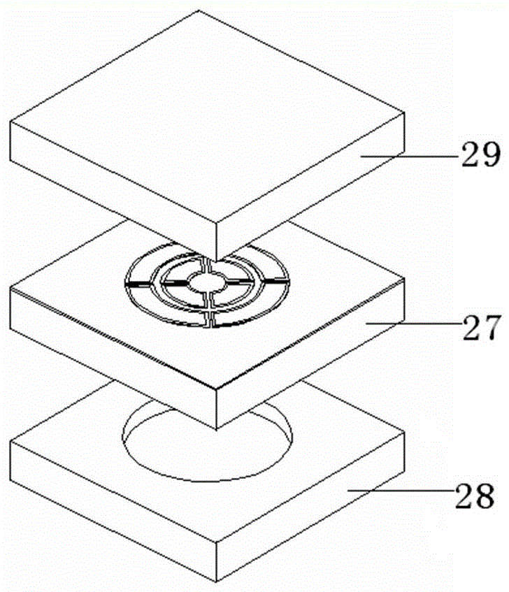
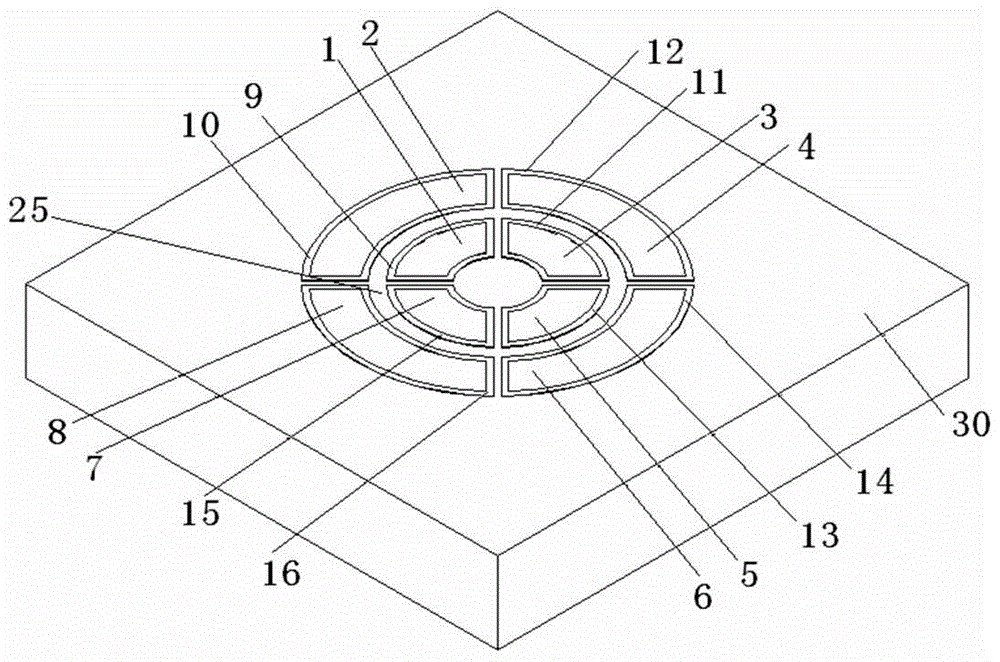
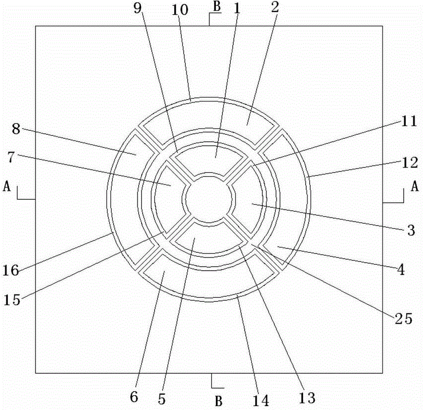
[0033] figure 1 It is an exploded view of the piezoelectric micro-acceleration sensor of the present invention, figure 2 It is a schematic structural diagram of the sensitive chip in the piezoelectric micro-acceleration sensor of the present invention, image 3 It is a top view of the sensitive chip in the piezoelectric micro-acceleration sensor of the present invention, Figure 4 for along image 3 Sectional drawing of A-A section line, Figure 5 for along image 3 Sectional drawing of the B-B section line, Image 6 It is a schematic diagram of the back of the sensitive chip in the piezoelectric micro-acceleration sensor of the present invention. exist Figure 1~6 Among them, the piezoelectric micro-acceleration sensor of the present invention includes a sensitive chip 27, an upper glass plate 29, and a lower glass plate 28; wherein, the sensitive chip 27 contains the first upper electrode 1, the second upper electrode 2, the third upper electrode 3, Fourth upper el...
Embodiment 2
[0048]The structure of this embodiment is the same as that of Embodiment 1, the difference is that the outer circle of the ring formed by the first piezoelectric layer, the third piezoelectric layer, the fifth piezoelectric layer and the seventh piezoelectric layer The diameter is 45 μm larger than the diameter of the outer circle of the ring formed by the first upper electrode, the third upper electrode, the fifth upper electrode, and the seventh upper electrode; the first piezoelectric layer, the third piezoelectric layer, the fifth The diameter of the inner circle of the ring formed by the piezoelectric layer and the seventh piezoelectric layer is 45 μm smaller than the diameter of the inner circle of the ring formed by the first upper electrode, the third upper electrode, the fifth upper electrode, and the seventh upper electrode; The diameter of the outer circle of the ring formed by the second piezoelectric layer, the fourth piezoelectric layer, the sixth piezoelectric la...
Embodiment 3
[0050] The structure of this embodiment is the same as that of Embodiment 1, the difference is that the outer circle of the ring formed by the first piezoelectric layer, the third piezoelectric layer, the fifth piezoelectric layer and the seventh piezoelectric layer The diameter is 40 μm larger than the diameter of the outer circle of the ring formed by the first upper electrode, the third upper electrode, the fifth upper electrode, and the seventh upper electrode; the first piezoelectric layer, the third piezoelectric layer, the fifth The diameter of the inner circle of the ring formed by the piezoelectric layer and the seventh piezoelectric layer is 40 μm smaller than the diameter of the inner circle of the ring formed by the first upper electrode, the third upper electrode, the fifth upper electrode, and the seventh upper electrode; The diameter of the outer circle of the ring formed by the second piezoelectric layer, the fourth piezoelectric layer, the sixth piezoelectric l...
PUM
 Abstract
Description
Claims
Application Information
 - R&D Engineer
- R&D Manager
- IP Professional
- Industry Leading Data Capabilities
- Powerful AI technology
- Patent DNA Extraction
Browse by: Latest US Patents, China's latest patents, Technical Efficacy Thesaurus, Application Domain, Technology Topic, Popular Technical Reports.
© 2024 PatSnap. All rights reserved.Legal|Privacy policy|Modern Slavery Act Transparency Statement|Sitemap|About US| Contact US: help@patsnap.com


