Back-contact back-junction solar battery three-dimension electrode and manufacturing method thereof
A technology of solar cells and three-dimensional electrodes, applied in the field of solar cells, can solve the problems of reduced battery performance, uncollected current, and high battery series resistance, and achieves the effects of reducing recombination rate, improving tolerance, and reducing series resistance.
- Summary
- Abstract
- Description
- Claims
- Application Information
AI Technical Summary
Problems solved by technology
Method used
Image
Examples
preparation example Construction
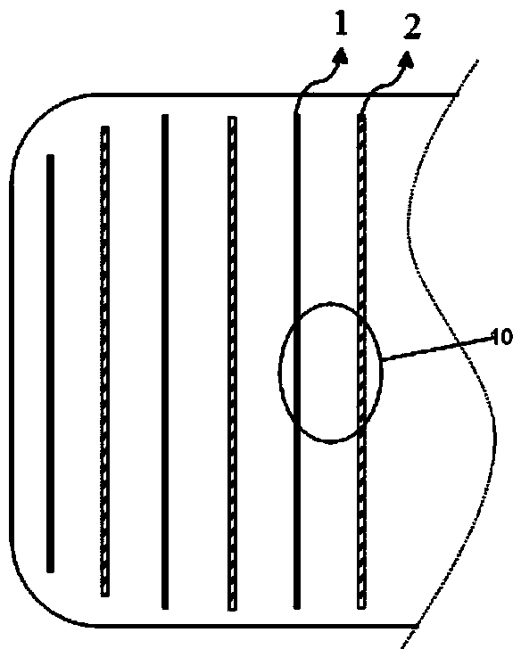
[0022] refer to Figure 1 to Figure 6 Describe the preparation method of above-mentioned electrode, its main steps are as follows:
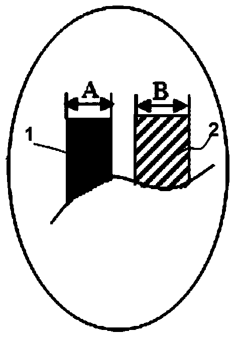
[0023] Deposit silver fine grid electrode 1 (i.e., negative electrode grid line) on the n+ area of the back junction-back junction contact solar cell, with an electrode width of A; deposit aluminum thin grid electrode 2 (i.e., positive electrode grid line) on the p+ area, with an electrode width of It is B, after sintering, the positive and negative fine grid electrodes arranged alternately in interdigitated shape on the back are obtained;
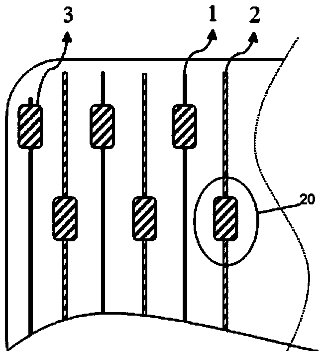
[0024] Deposit insulating ink 3 on the negative electrode fine grid where the positive electrode main grid needs to be prepared on the back of the battery. The thickness of the deposited ink is 10-30 μm, the width of the ink is C, and the length is D, and the ink width C is greater than the width A of the silver fine grid electrode;
[0025] Deposit insulating ink 3 on the positive electrode fine grid wher...
Embodiment 1
[0031] N-type monocrystalline silicon wafers of 1-3.5Ω·cm are used, and the preparation steps are as follows:
[0032] Step 1. Print silver fine grid electrodes with a width of 150 μm on the n+ area on the back of the silicon wafer, and print aluminum fine grid electrodes with a width of 250 μm on the p+ area, and put them into a sintering furnace for sintering;
[0033] Step 2. Use accurate alignment screen printing to print insulating ink on the negative electrode fine grid where the positive electrode main grid needs to be prepared on the back. The thickness of the printing ink is 20 μm, the width of the printing ink is 300 μm, and the length is 1.5 mm; Bit screen printing, printing insulating ink on the positive electrode fine grid where the negative electrode main grid needs to be prepared on the back, the thickness of the printing ink is 20 μm, the width of the printing ink is 300 μm, and the length is 1.5 mm; put the above silicon wafer into the drying furnace Dry in me...
PUM
 Abstract
Description
Claims
Application Information
 - R&D
- Intellectual Property
- Life Sciences
- Materials
- Tech Scout
- Unparalleled Data Quality
- Higher Quality Content
- 60% Fewer Hallucinations
Browse by: Latest US Patents, China's latest patents, Technical Efficacy Thesaurus, Application Domain, Technology Topic, Popular Technical Reports.
© 2025 PatSnap. All rights reserved.Legal|Privacy policy|Modern Slavery Act Transparency Statement|Sitemap|About US| Contact US: help@patsnap.com


