Method for manufacturing polycrystalline silicon with growth directions controllable

A technology of polysilicon growth and production method, which is applied in semiconductor/solid-state device manufacturing, electrical components, circuits, etc., and can solve problems such as the inability to effectively control the growth direction of polysilicon 600, the inability to effectively control the area, etc.

Active Publication Date: 2014-02-19
TCL CHINA STAR OPTOELECTRONICS TECH CO LTD
View PDF3 Cites 4 Cited by
  • Summary
  • Abstract
  • Description
  • Claims
  • Application Information

AI Technical Summary

Problems solved by technology

Although the above manufacturing method can optimize the crystallization effect by adjusting the parameters of the laser, it cannot effectively control the growth direction of the polysilicon 600 during the annealing process, and thus cannot effectively control the region where the grain boundary appears

Method used


Image

  • Method for manufacturing polycrystalline silicon with growth directions controllable
  • Method for manufacturing polycrystalline silicon with growth directions controllable
  • Method for manufacturing polycrystalline silicon with growth directions controllable

Examples


Embodiment Construction

[0036] In order to further illustrate the technical means adopted by the present invention and its effects, the following describes in detail in conjunction with preferred embodiments of the present invention and accompanying drawings.

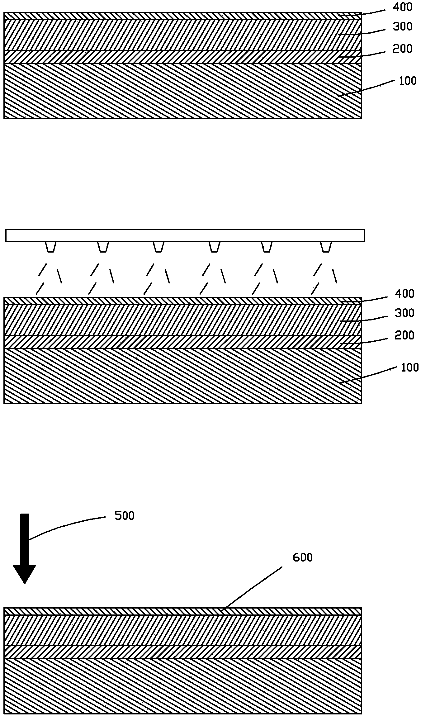
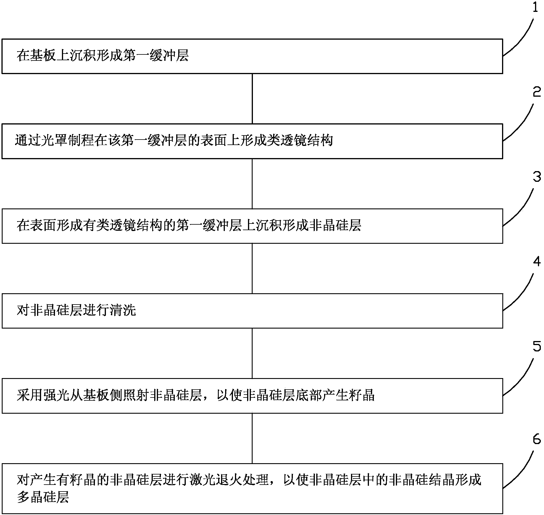
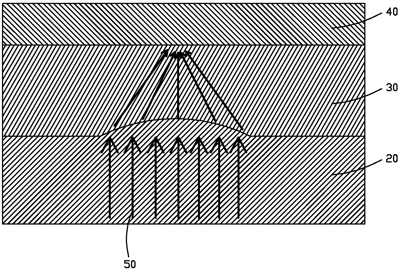
[0037] see Figure 2 to Figure 10 , the present invention provides a polysilicon production method capable of controlling the growth direction of polysilicon, comprising the following steps:

[0038] Step 1, depositing and forming a first buffer layer 20 on the substrate 10 .

[0039] The refractive index of the first buffer layer 20 is 1.7-2.1. In this embodiment, the refractive index of the first buffer layer 20 is preferably 1.9. Further, the first buffer layer 20 is made of silicon nitride (SiN x ) formed by deposition.

[0040] The substrate 10 is a glass substrate or a plastic substrate.

[0041] Step 2, forming a lens-like structure 22 on the surface of the first buffer layer 20 through a photomask process.

[0042] In this step, r...


PUM

PropertyMeasurementUnit
Wavelengthaaaaaaaaaa

Abstract

The invention provides a method for manufacturing polycrystalline silicon with growth directions controllable. The method includes the following steps that firstly, a first buffering layer (20) is deposited on a substrate (10); secondly, a lens-like structure (22) is formed on the surface of the first buffering layer (20) through photomask manufacturing; thirdly, an amorphous silicon layer (40) is deposited on the first buffering layer (20) with the lens-like structure (22) formed on the surface; fourthly, the amorphous silicon layer (40) is cleaned; fifthly, the amorphous silicon layer (40) is illuminated through hard light (50) from the substrate (10) to make seed crystals generated at the bottom of the amorphous silicon layer (40); sixthly, the amorphous silicon layer (40) with the generated seed crystals is subject to laser annealing treatment to make amorphous silicon in the amorphous silicon layer (40) crystallized so as to form a polycrystalline silicon layer (70). The growth directions of the polycrystalline silicon can be controlled through the method.

Description

technical field [0001] The invention relates to the field of display technology, in particular to a polysilicon manufacturing method capable of controlling the growth direction of polysilicon. Background technique [0002] In recent years, the display technology has developed rapidly, and the flat panel display is very different from the traditional video image display with its completely different display and manufacturing technology. The traditional video image display is mainly cathode ray tube CRT (Cathode ray tubes); the main difference between the flat panel display is the change in weight and volume (thickness), usually the thickness of the flat panel display does not exceed 10cm, of course there are other Different, such as display principles, manufacturing materials, processes, and various technologies in video image display drivers. [0003] Flat panel displays have the characteristics of complete planarization, lightness, thinness, and power saving, and are devel...

Claims


Application Information

Patent Timeline
IPC IPC(8): H01L21/3205
CPCH01L21/02675H01L21/02422H01L21/02532H01L21/02488H01L21/02502
Inventor 张翔
Owner TCL CHINA STAR OPTOELECTRONICS TECH CO LTD
Why Eureka
Try Eureka