Infrared detector structure for improving spectral flatness

An infrared detector and flatness technology, applied in semiconductor devices, electrical components, circuits, etc., can solve the problems of unsatisfactory response flatness, not taking into account the fluctuation of infrared photons, and the influence of light field distribution in photosensitive areas, etc. Good flatness, structure and the effect of simple process

Inactive Publication Date: 2014-02-12
SHANGHAI INST OF TECHNICAL PHYSICS - CHINESE ACAD OF SCI
View PDF4 Cites 2 Cited by
  • Summary
  • Abstract
  • Description
  • Claims
  • Application Information

AI Technical Summary

Problems solved by technology

Depend on figure 1 (a) It can be seen that the peak response wavelength of the device is greater than 10 microns, and the response curve becomes curved near the peak; after the antireflection film is grown on the photosensitive surface of the device, the flatness of the response near the peak can be improved (such as figure 1 (b)); but in its response band, as the wavelength increases, the flatness of the response is far from ideal
The reason is that the fluctuation of infrared photons is not considered, and it is not realized that the non-light-sensitive area will also have a greater impact on the light field distribution of the light-sensitive area.

Method used


Image

  • Infrared detector structure for improving spectral flatness
  • Infrared detector structure for improving spectral flatness
  • Infrared detector structure for improving spectral flatness

Examples


Embodiment Construction

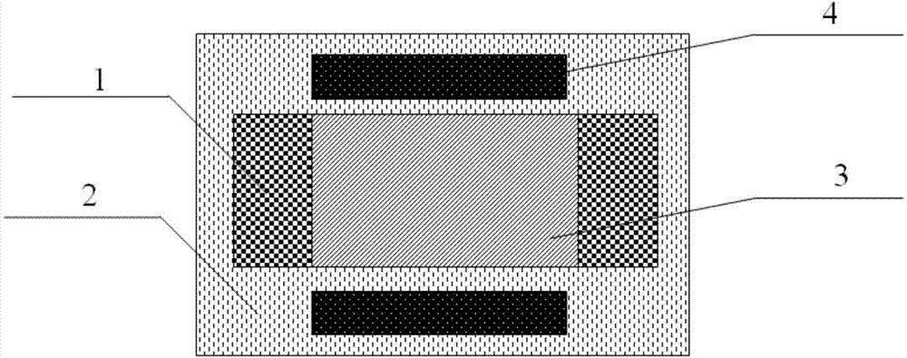
[0033] Combine below figure 2 Specific embodiments of the present invention will be described in detail.

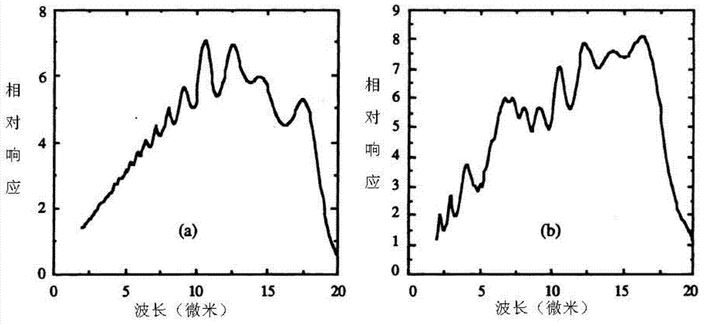
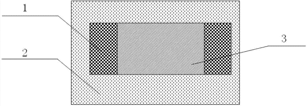
[0034] 1. The distance between the photosensitive area 3 and other dielectric areas 4 generally does not exceed the peak wavelength of the infrared detector response, and within the range allowed by the lithography precision and process conditions, the smaller the better.

[0035] 2. For other dielectric regions 4, in practice, the same material as that of the photosensitive region 3 is generally selected, for example, both are HgCdTe materials, and anti-reflection coatings with the same thickness and medium are grown on the surfaces of the photosensitive region 3 and other dielectric regions 4 , and then use an etching or etching process for electrical isolation. In this way, the reflection of infrared photons on the surface of the photosensitive area 3 and other medium areas 4 and the interference phenomenon between them are greatly weakened.

[0036] 3. The geometri...


PUM


Abstract

The invention discloses an infrared detector structure for improving response spectral flatness. The infrared detector structure for improving the spectral flatness comprises metal electrodes, a substrate, a photosensitive area and other media. The metal electrodes are located on the left side and the right side of the rectangular photosensitive area. The other media are located on the upper side and the lower side of the rectangular photosensitive area. The other media are the same as the photosensitive area in material and are electrically isolated from the metal electrodes and the photosensitive area. The infrared detector structure is simple and effective, non-linear response spectral shapes are eliminated, and the spectral flatness is improved.

Description

technical field [0001] The invention relates to a structure of an infrared detector, in particular to an infrared detector structure and a preparation method for improving the flatness of a response spectrum. Background technique [0002] Modern infrared detection technology is of great significance to the development of national economy and society. With the continuous development of remote sensing instrument technology, it has developed from point target detection, scanning imaging, and multispectral scanning imaging to hyperspectral imaging. Focal planes, multi-band infrared focal planes, and smart integrated detector components are developing. On the one hand, infrared detectors play an irreplaceable role in earth observation. On the other hand, the device center distance of the infrared focal plane chip has moved from hundreds of microns to tens or even tens of microns. When the device structure size is close to or within an order of magnitude of the photon wavelengt...

Claims


Application Information

Patent Timeline
Patent Type & Authority Applications(China)
IPC IPC(8): H01L31/09H01L27/146
CPCH01L31/09H01L31/022408
Inventor 许金通李向阳朱龙源王妮丽储开慧赵水平兰添翼
Owner SHANGHAI INST OF TECHNICAL PHYSICS - CHINESE ACAD OF SCI
Why Eureka
Try Eureka