


Quick Research
Generate reliable direction feasibility study reports for your R&D in just a few steps.

Technical Q&A
Discover and master advanced knowledge NOW. Basics, ideas, possibilities, all at once.

Find Solutions
As an expert in R&D theories, this can generate solutions to your technical problems instantly.

Evaluate Feasibility
Analyze your overall solution with one click, know your potential R&D risks in advance.

Monitor Landscape
Get weekly tech updates, stay abreast of the latest tech innovations and key insights.
Semiconductor element, integrated circuit, manufacturing method of semiconductor element and integrated circuit and electronic device
A technology of integrated circuits and manufacturing methods, which is applied in semiconductor/solid-state device manufacturing, semiconductor devices, circuits, etc., and can solve problems such as device narrow channel effects, electric field concentration in the edge region of devices, and transistor threshold voltage increase.
- Summary
- Abstract
- Description
- Claims
- Application Information
AI Technical Summary
Problems solved by technology
Method used
Image

Examples
Embodiment 1
[0046] An embodiment of the present invention provides a semiconductor device, which can effectively reduce the short channel effect.
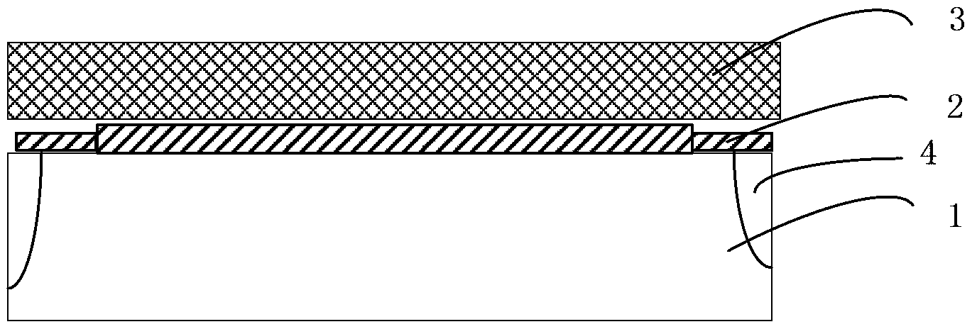
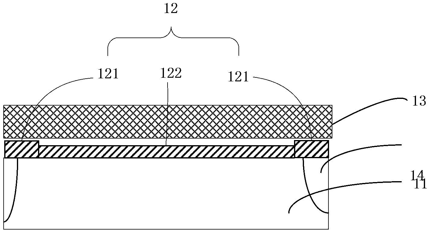
[0047] figure 2 It is a schematic structural diagram of a semiconductor device according to an embodiment of the present invention (a cross-sectional view along the width direction of a gate). Depend on figure 2It can be seen that the semiconductor device in this embodiment includes a semiconductor substrate 11, and a gate oxide layer 12 and a gate 13 located on the semiconductor substrate 11, wherein the gate oxide layer 12 of the semiconductor device includes two parts, respectively the first part A gate oxide layer 121 and a second part of the gate oxide layer 122, the first part of the gate oxide layer 121 is located in the width edge region of the gate 13, and the second part of the gate oxide layer 122 is located in the middle region of the gate 13; and, the first part of the gate oxide layer The thickness of the gate oxide layer 121...
Embodiment 2
[0052] An embodiment of the present invention provides an integrated circuit, which can effectively reduce the short channel effect.
[0053] The integrated circuit provided by the embodiment of the present invention includes a semiconductor substrate, and a core device and an input / output device formed on the semiconductor substrate. The core device is located in the core device region (core device region) on the semiconductor substrate, and the input and output devices are located in the input and output device region (I / O device region) on the semiconductor substrate. Wherein, in the core device area of the integrated circuit, various semiconductor devices as described in Embodiment 1 are formed, that is, the core device includes various semiconductor devices described in Embodiment 1.
[0054] Specifically, in this embodiment, the structure of the core device can refer to figure 2 , the gate oxide layer 12 includes two parts, namely a first part of the gate oxide layer...
Embodiment 3
[0064] An embodiment of the present invention provides a method for manufacturing a semiconductor device, which can be used to manufacture the semiconductor device described in Embodiment 1. Next, the detailed steps of the manufacturing method of the semiconductor device proposed by the embodiment of the present invention are described as follows:
[0065] Step 1. Provide a semiconductor substrate;
[0066] This step is exactly the same as the corresponding step in the method for manufacturing a semiconductor device in the prior art. The constituent material of the semiconductor substrate may be undoped single crystal silicon, single crystal silicon doped with impurities, silicon on insulator (SOI) and the like.
[0067] Step 2. Forming a gate oxide layer on the semiconductor substrate, the gate oxide layer includes two parts, respectively a first part of the gate oxide layer located in the width edge region of the gate and a second part of the gate oxide layer located in the...
PUM
 Abstract
Description
Claims
Application Information
 - R&D Engineer
- R&D Manager
- IP Professional
- Industry Leading Data Capabilities
- Powerful AI technology
- Patent DNA Extraction
Browse by: Latest US Patents, China's latest patents, Technical Efficacy Thesaurus, Application Domain, Technology Topic, Popular Technical Reports.
© 2024 PatSnap. All rights reserved.Legal|Privacy policy|Modern Slavery Act Transparency Statement|Sitemap|About US| Contact US: help@patsnap.com