Quantum dot stacking structure and manufacturing method thereof and light emitting component
A technology of stacking structure and light-emitting elements, applied in electrical components, semiconductor devices, circuits, etc., can solve the problems of poor light conversion efficiency, self-aggregation, uneven thickness, etc.
- Summary
- Abstract
- Description
- Claims
- Application Information
AI Technical Summary
Problems solved by technology
Method used
Image
Examples
Embodiment Construction
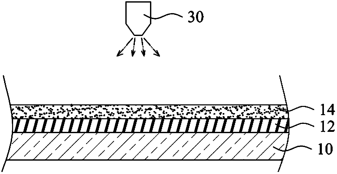
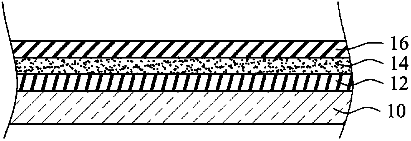
[0030] reference Figure 1 to Figure 7 , Showing a schematic diagram of an embodiment of the method for manufacturing the quantum dot stack structure of the present invention. reference figure 1 , Provide a substrate layer 10. The substrate layer 10 is made of a light-transmissive material. In this embodiment, the substrate layer 10 is glass; however, in other embodiments, the substrate layer 10 may also be made of plastic or other flexible materials. Next, a bottom spacer layer 12 is formed on the substrate layer 10. The bottom spacer layer 12 is made of a flexible and light-permeable material, and contains a polymer silicon oxide compound. In this embodiment, the polymer silicon-oxygen compound contains a methyl group, for example, poly-dimethylsiloxane (PDMS). In addition, the bottom spacer layer 12 has the characteristics of low surface tension. Preferably, the surface tension is lower than 30 dyne / cm. In this embodiment, the bottom spacer layer 12 is a film, which is at...
PUM
 Abstract
Description
Claims
Application Information
 - R&D
- Intellectual Property
- Life Sciences
- Materials
- Tech Scout
- Unparalleled Data Quality
- Higher Quality Content
- 60% Fewer Hallucinations
Browse by: Latest US Patents, China's latest patents, Technical Efficacy Thesaurus, Application Domain, Technology Topic, Popular Technical Reports.
© 2025 PatSnap. All rights reserved.Legal|Privacy policy|Modern Slavery Act Transparency Statement|Sitemap|About US| Contact US: help@patsnap.com


