pmos transistor and method of forming the same

A technique for transistors and manufacturing methods, applied in the field of PMOS transistors and their manufacture, capable of solving problems affecting circuit performance, PMOS transistors cannot effectively overcome thermal electron effects, etc., achieving the effect of improving circuit performance and overcoming thermal electron effects

Active Publication Date: 2016-02-17
SEMICON MFG INT (SHANGHAI) CORP
View PDF5 Cites 0 Cited by
  • Summary
  • Abstract
  • Description
  • Claims
  • Application Information

AI Technical Summary

Problems solved by technology

[0008] combine figure 1 , figure 2 and image 3 As shown, when the tip depth H is small, figure 1 The lightly doped drain structure 5 will be removed a lot, so that the PMOS transistor cannot effectively overcome the hot electron effect, which affects the performance of the circuit

Method used


Image

  • pmos transistor and method of forming the same
  • pmos transistor and method of forming the same
  • pmos transistor and method of forming the same

Examples


Embodiment Construction

[0058] The technical solution of the present invention will be described clearly and completely through specific embodiments below in conjunction with the accompanying drawings. Apparently, the described embodiments are only a part of the possible implementation modes of the present invention, not all of them. According to these embodiments, all other implementation manners that can be obtained by those skilled in the art without creative efforts belong to the protection scope of the present invention.

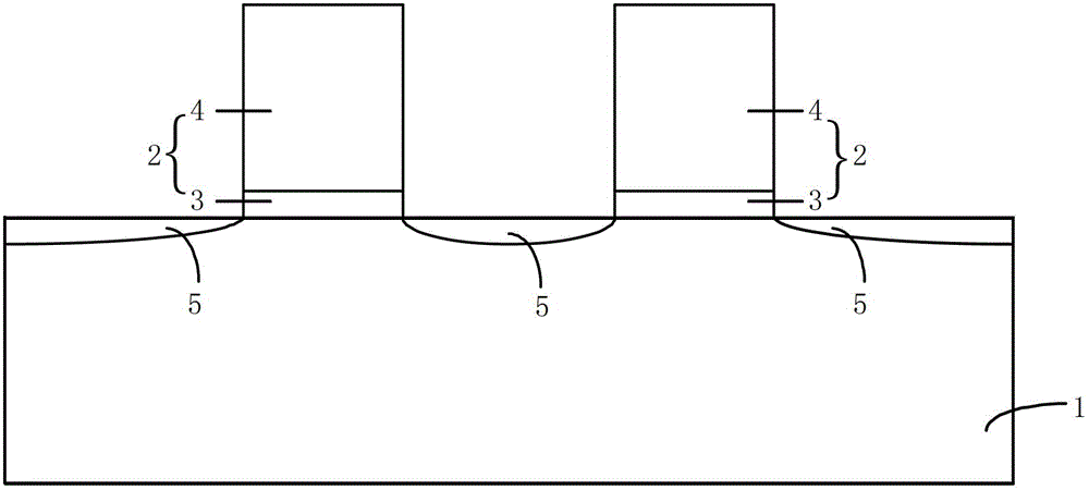
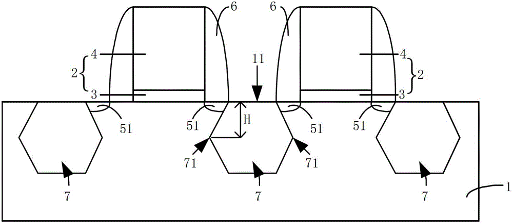
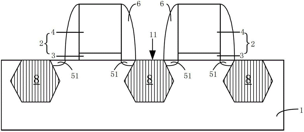
[0059] Figure 4 It is the fabrication flowchart of the PMOS transistor in the embodiment of the PMOS transistor fabrication method of the present invention, Figure 5 to Figure 22 It is a cross-sectional view of a PMOS transistor at different manufacturing stages in an embodiment of the PMOS transistor manufacturing method of the present invention, and the following will Figure 5 to Figure 22 and Figure 4 Together, the method for manufacturing the PMOS transistor of the p...


PUM


Abstract

Provided are a P-channel Metal Oxide Semiconductor (PMOS) transistor and a forming method thereof. The forming method includes forming gate structures on a monocrystalline silicon substrate, wherein the gate structures comprise gate dielectric layers and gate electrodes; forming lightly doped drain structures located on two sides of the gate structures on the substrate; forming first side walls on two sides of the gate structures; forming second side walls on two sides of the gate structures, wherein the first side walls are located between the gate structures and the second side walls; forming sigma-shaped first grooves in the substrate in the areas where the source electrode and the source electrode are pre-formed with the gate structures, the first side walls and the second side walls serving as masks; forming silicon-germanium materials in the first grooves. After the second side walls are arranged on two sides of the gate structures, the distance between the groove tips of the first grooves and the surface of the substrate is increased, little lightly doped drain structures are removed while many lightly doped drain structures are reserved, accordingly the hot electron effect can be effectively overcome and the circuit performance can be improved.

Description

technical field [0001] The invention belongs to the field of semiconductor manufacturing, in particular to a PMOS transistor and a manufacturing method thereof. Background technique [0002] In the existing manufacturing process of semiconductor devices, since stress can change the energy gap and carrier mobility of silicon materials, it has become an increasingly common means to improve the performance of MOS transistors through stress. Specifically, by properly controlling the stress, the mobility of carriers (electrons in NMOS transistors and holes in PMOS transistors) can be increased, thereby increasing the driving current, thereby greatly improving the performance of MOS transistors. For PMOS transistors, embedded silicon germanium technology (Embedded SiGe Technology) can be used to generate compressive stress in the channel region of the transistor, thereby improving carrier mobility. The so-called embedded silicon germanium technology refers to embedding silicon ge...

Claims


Application Information

Patent Timeline
Patent Type & Authority Patents(China)
IPC IPC(8): H01L21/336H01L29/78H01L29/06
CPCH01L21/823468H01L27/092H01L29/6656H01L29/78
Inventor 韩秋华隋运奇
Owner SEMICON MFG INT (SHANGHAI) CORP
Why Eureka
Try Eureka