Liquid crystal display device
A liquid crystal display device and display area technology, applied in nonlinear optics, instruments, optics, etc., can solve the problems of reduced aperture ratio and transmittance, reduced contrast, insufficient utilization of transmission area, etc. Effect
- Summary
- Abstract
- Description
- Claims
- Application Information
AI Technical Summary
Problems solved by technology
Method used
Image
Examples
Embodiment 1
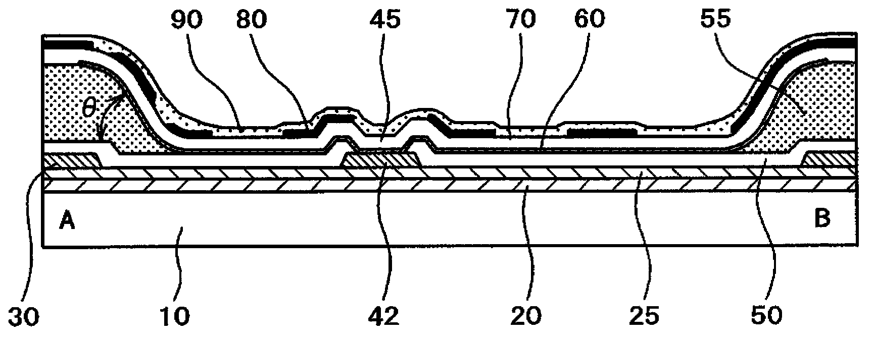
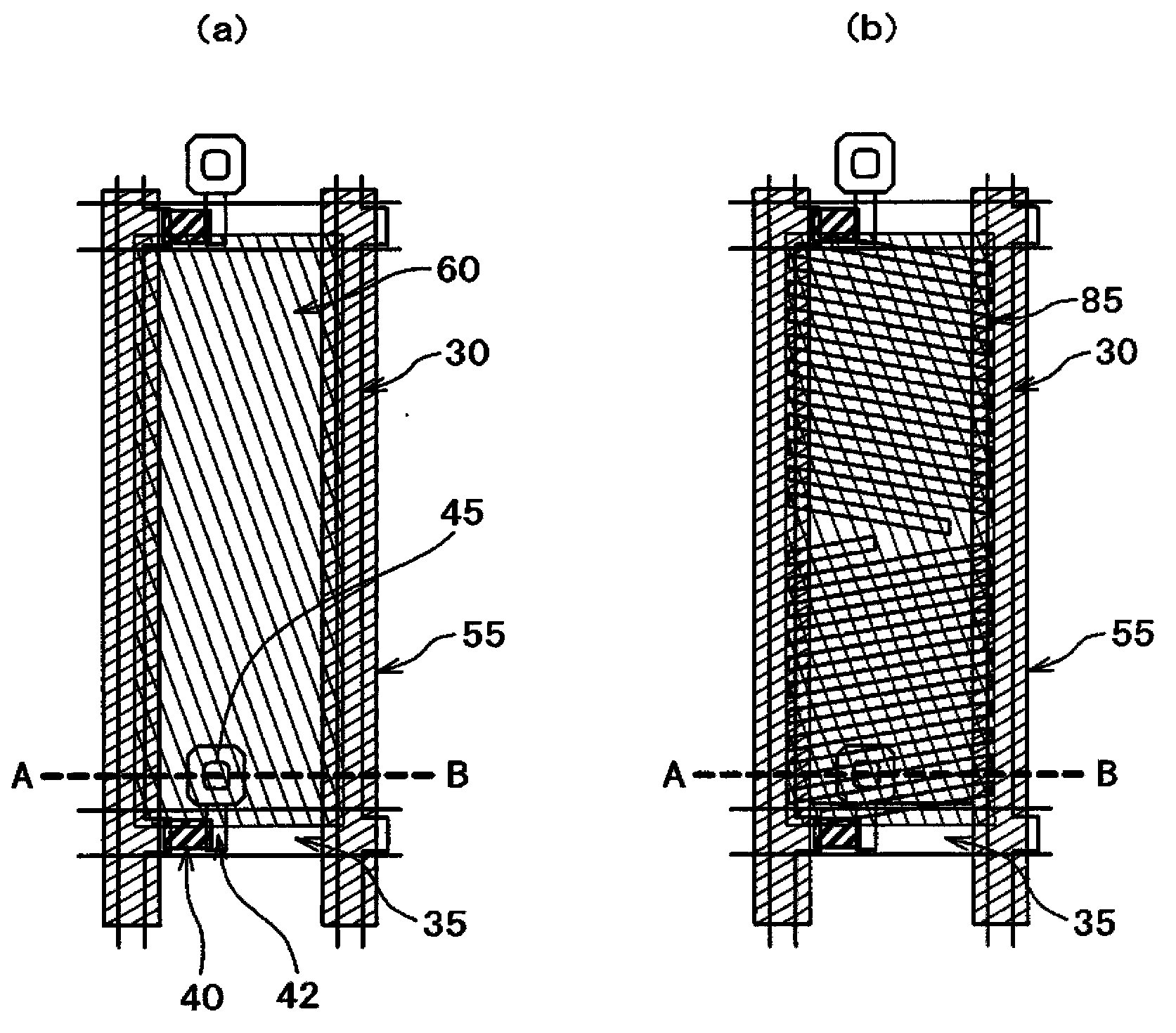
[0079] figure 1 and figure 2 The liquid crystal display device of Example 1 is shown. figure 2 represents the floor plan of a pixel, figure 1 express figure 2 A-B cross-sectional view of one pixel is shown. figure 2 middle, figure 2 (a) shows a plan view from a drain wiring, a gate wiring to a pixel electrode, figure 2 (b) shows a plan view up to the uppermost common electrode. Example 1 is an example in which most of the organic insulating film in the pixel is removed while leaving the organic insulating film on the drain wiring.
[0080] figure 1 Among them, an insulating film 20 and an insulating film 25 are formed on a TFT substrate 10 made of transparent glass, and a drain wiring 30 and a source electrode 42 of a TFT 40 are formed on the insulating film 25 . In addition, if figure 2 As shown, a gate wiring 35 is formed between the insulating film 20 and the insulating film 25 .
[0081] An inorganic insulating film 50 is formed over the entire surface of ...
Embodiment 2
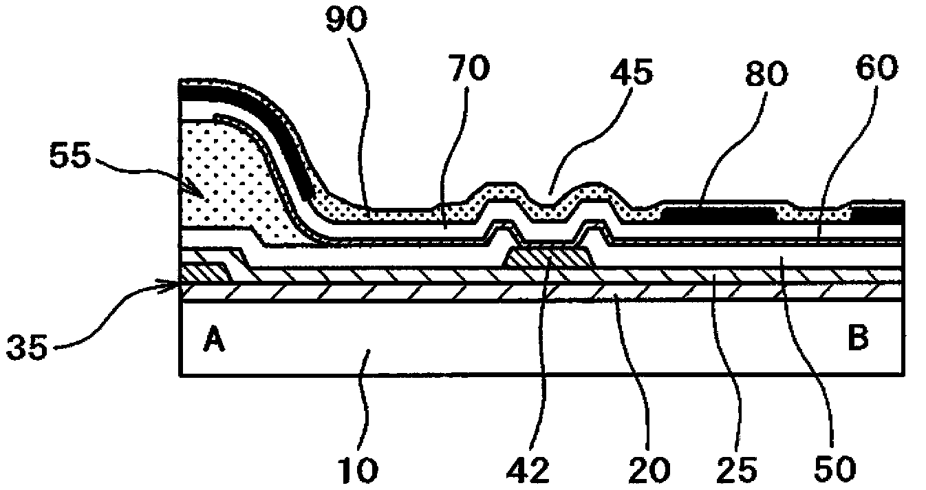
[0091] image 3 and Figure 4 The liquid crystal display device of Example 2 is shown. Figure 4 represents the floor plan of a pixel, image 3 express Figure 4 The A-B cross-sectional view of a pixel is shown. Figure 4 middle, Figure 4 (a) shows a plan view from the drain line, the gate line to the pixel electrode, Figure 4 (b) shows a plan view up to the uppermost common electrode. Example 2 is an example in which most of the organic insulating film in the pixel is removed while leaving the organic insulating film on the gate wiring.
[0092] In this example, in Figure 4 In this method, the organic insulating film 55 with a film thickness of about 2 μm is patterned on the upper portion of the gate wiring 35 formed in the lateral direction, and the annealing treatment is performed to form the off angle of the end of the organic insulating film to, for example, about 40°. Spend. A transparent pixel electrode (first electrode) 60 is provided thereon so as to be el...
Embodiment 3
[0097] Figure 5 and Image 6 The liquid crystal display device of Example 3 is shown. Image 6 represents the floor plan of a pixel, Figure 5 express Image 6 The A-B cross-sectional view of a pixel is shown. Image 6 middle, Image 6 (a) shows a plan view from the drain wiring, the gate wiring to the common electrode, Image 6 (b) shows a plan view up to the uppermost pixel electrode. Example 3 is an example in which most of the organic insulating film in the pixel is removed while leaving the organic insulating film on the gate wiring.
[0098] In Example 3, such as Image 6 As shown, common electrode wiring 37 is provided in the lateral direction, and is electrically connected to the common electrode through a contact hole. In the same manner as in Example 2, an organic insulating film 55 with a film thickness of about 2 μm is patterned on top of the gate wiring 35 and annealed, whereby the inclination angle θ at the end of the organic insulating film 55 is formed...
PUM
| Property | Measurement | Unit |
|---|---|---|
| thickness | aaaaa | aaaaa |
Abstract
Description
Claims
Application Information
 - R&D
- Intellectual Property
- Life Sciences
- Materials
- Tech Scout
- Unparalleled Data Quality
- Higher Quality Content
- 60% Fewer Hallucinations
Browse by: Latest US Patents, China's latest patents, Technical Efficacy Thesaurus, Application Domain, Technology Topic, Popular Technical Reports.
© 2025 PatSnap. All rights reserved.Legal|Privacy policy|Modern Slavery Act Transparency Statement|Sitemap|About US| Contact US: help@patsnap.com


