Organic semiconductor material, its preparation method and application
An organic semiconductor, coupling reaction technology, applied in the fields of semiconductor/solid-state device manufacturing, semiconductor devices, luminescent materials, etc., can solve the problems of molecular structure changes, affecting the stability and performance of devices, and achieve large modification space and flexible synthesis routes. , the effect of good solution processability
- Summary
- Abstract
- Description
- Claims
- Application Information
AI Technical Summary
Problems solved by technology
Method used
Image


Examples
preparation example Construction
[0053] As one of the more preferred embodiments, the preparation method may include:
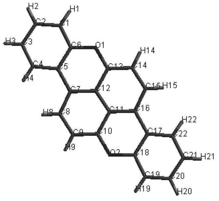
[0054] Direct halogenation of 2,6-dialkylnaphthalene followed by a transition metal-catalyzed coupling reaction yielded a 1,5-diarylnaphthalene-based compound containing a phenolic hydroxyl group, followed by microwave-assisted synthesis of o-dichlorobenzene The organic semiconductor material is obtained by performing a ring-closing reaction as a solvent.
[0055] In the present invention, the aromatic group Ar is used as a bridge, and the active group is introduced into the reactive site on the Ar group to solve the solubility and chemical modification problems of this type of compound and expand the reactivity of the structure of this type of compound. According to the application, a series of oxygen-bridged 1,5-diarylnaphthalene-based optoelectronic materials can be obtained, which can be widely used in the fields of organic electronics such as organic electroluminescence, organic field e...
Embodiment 1 2
[0059] The preparation process of embodiment 1 dioxaanthanthrene, comprising:
[0060] Preparation of A, 2,2'-(1,5-naphthyl)diphenol (compound a)
[0061]
[0062] In a 250mL two-neck round bottom flask, add 3g of 1,5-dibromonaphthalene, 5g of 2-hydroxyphenylboronic acid, 0.6g of tetrakistriphenylphosphopalladium, 5.8g of potassium carbonate, 60mL of toluene and 6mL of water. The system was degassed with a vacuum pump for half an hour, and then filled with nitrogen. The reaction was refluxed overnight, and the solution was cooled to room temperature after the reaction was terminated. The organic phase was collected by liquid separation through a separatory funnel, the aqueous phase was extracted three times with ethyl acetate, and the organic phases were combined. Dry with anhydrous sodium sulfate, filter, spin dry the solvent, and separate by column chromatography to obtain a white solid with a yield of 85%. 1 HNMR (CDCl 3 , 500MHz): δ=7.68(d, 2H), 7.49-7.44(m, 4H), 7....
Embodiment 23
[0066] Embodiment 23, the preparation method of 10-diphenyldioxaanthanthrene, comprising:
[0067] The preparation of A, 1,5-two (pinacol borate) naphthalene:
[0068]
[0069] Dissolve 6.86g of 1,5-dibromonaphthalene in 100mL of anhydrous N,N-dimethylformamide, then add 18.3g of biboronic acid pinacol ester, 1.75g of [1,1'-bis(diphenylphosphine Base) ferrocene] palladium dichloride and 9.42g potassium acetate. The system was reacted overnight at 90°C under the protection of nitrogen, and poured into ice water after the reaction was terminated. The precipitate was filtered off, washed with ethanol, and dried in vacuo to give a white solid with a yield of 88%. 1 HNMR (CDCl 3 , 500MHz): δ=8.89(d, 2H), 8.07(d, 2H), 7.52(t, 2H), 1.42(s, 24H).
[0070] The preparation of B, 2-bromo-4-phenylphenol:
[0071]
[0072] 7.63g of 4-phenylphenol was dissolved in 50mL of chloroform, and then 10mL of chloroform dissolved in 2.63mL of liquid bromine was added dropwise. The syst...
PUM
 Abstract
Description
Claims
Application Information
 - R&D
- Intellectual Property
- Life Sciences
- Materials
- Tech Scout
- Unparalleled Data Quality
- Higher Quality Content
- 60% Fewer Hallucinations
Browse by: Latest US Patents, China's latest patents, Technical Efficacy Thesaurus, Application Domain, Technology Topic, Popular Technical Reports.
© 2025 PatSnap. All rights reserved.Legal|Privacy policy|Modern Slavery Act Transparency Statement|Sitemap|About US| Contact US: help@patsnap.com