A kind of array substrate and its manufacturing method and display panel

A technology of an array substrate and a manufacturing method, which is applied in the field of liquid crystal display, can solve problems such as poor display, and achieve the effects of not being easily broken, improving picture display quality, and enhancing display effect.

Inactive Publication Date: 2015-08-26
BEIJING BOE OPTOELECTRONCIS TECH CO LTD
View PDF3 Cites 0 Cited by
  • Summary
  • Abstract
  • Description
  • Claims
  • Application Information

AI Technical Summary

Problems solved by technology

[0004] Embodiments of the present invention provide an array substrate, a manufacturing method thereof, and a display panel, which are used to solve the problem of bad display caused by damaged spacers in the prior art and improve the display effect of a liquid crystal display device

Method used


Image

  • A kind of array substrate and its manufacturing method and display panel
  • A kind of array substrate and its manufacturing method and display panel
  • A kind of array substrate and its manufacturing method and display panel

Examples


Embodiment Construction

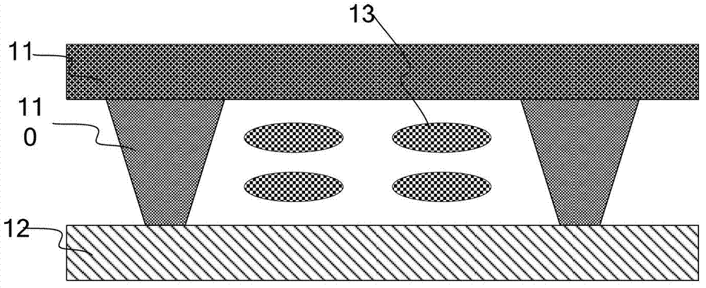
[0026] Embodiments of the present invention provide an array substrate, a manufacturing method thereof, and a display panel, which are used to solve the problem of poor display caused by damaged spacers in the prior art and improve the display effect of a liquid crystal display device.

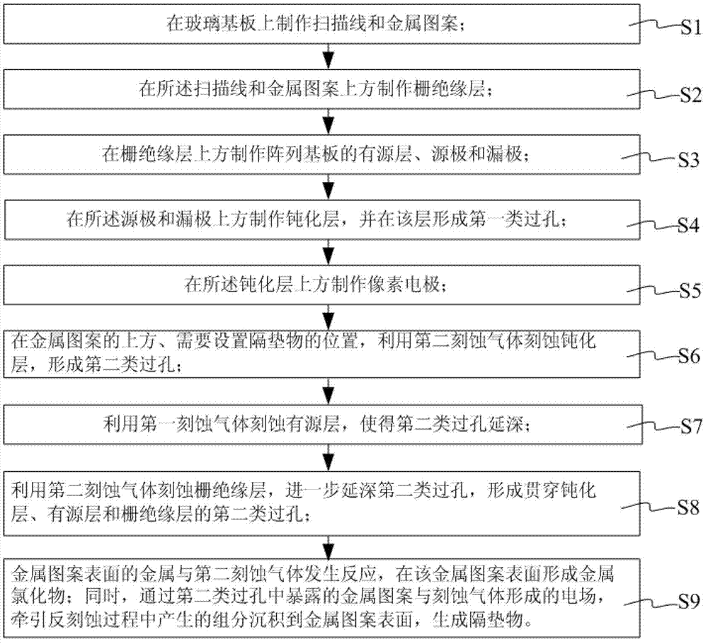
[0027] An embodiment of the present invention provides a method for manufacturing an array substrate, the method comprising:

[0028] forming patterns including scanning lines and spacer substrates in the same layer on the base substrate;

[0029] forming a gate insulating layer on the substrate after the aforementioned steps;

[0030] Forming a semiconductor thin film, a doped semiconductor thin film, and a source-drain metal thin film on the substrate that has completed the preceding steps, and forming a pattern including an active layer, a data line, a source electrode, and a drain electrode through a patterning process;

[0031] forming a passivation layer on the substrate having complete...


PUM


Abstract

An array substrate, a manufacturing method therefor, and a display panel. The manufacturing method comprises: forming a pattern comprises a scanning line (32) and a spacer base material (33) on a base substrate (31); forming a gate insulation layer (34); forming a pattern comprising an active layer (35), a data line, a source electrode and a drain electrode; forming a passivation layer (36); separately etching the passivation layer (36) and the gate insulation layer (34) by using a dry etching method, so as to form a via hole (38) for exposing the spacer base material (33), and by means of an electric field formed by using the spacer base material (33) exposed in the via hole (38) and etching gas used in the etching process, inducing a substance generated in the etching process in a reaction chamber to be deposited on a surface of the spacer base material (33), so as to generate a spacer (39).

Description

technical field [0001] The invention relates to the technical field of liquid crystal display, in particular to an array substrate, a manufacturing method thereof, and a display panel. Background technique [0002] With the development of thin film transistor liquid crystal display (TFT-LCD Display) technology and the progress of industrial technology, the production cost of liquid crystal display devices has been reduced, and the manufacturing process has been improved day by day. Mainstream technology; due to its own advantages, it has become an ideal display device in the minds of the market and consumers. At present, the stereoscopic display technology is increasingly emerging in the market, so it is increasingly important to solve the technical shortcomings of the stereoscopic display technology and improve the image quality (such as reducing color shift, reducing stereoscopic crosstalk, screen flicker, increasing viewing angle, etc.). [0003] Advanced ultra-dimension...

Claims


Application Information

Patent Timeline
Patent Type & Authority Patents(China)
IPC IPC(8): H01L21/77H01L27/12G02F1/1362G02F1/1368
CPCH01L21/77H01L27/12G02F1/13394H01L21/32136H01L27/1248H01L27/124H01L21/31116H01L27/1259H01L21/3065
Inventor 郭建
Owner BEIJING BOE OPTOELECTRONCIS TECH CO LTD
Why Eureka
Try Eureka