Elastic base/back surface line leading-based micro-electromechanical systems probe card and preparation method thereof
A micro-electromechanical system and probe card technology, which is applied in the direction of measuring electricity, measuring electrical variables, and manufacturing measuring instruments, etc., can solve the problems of low yield and long connecting line, etc. The effect of short circuit length
- Summary
- Abstract
- Description
- Claims
- Application Information
AI Technical Summary
Problems solved by technology
Method used
Image

Examples
Embodiment 1
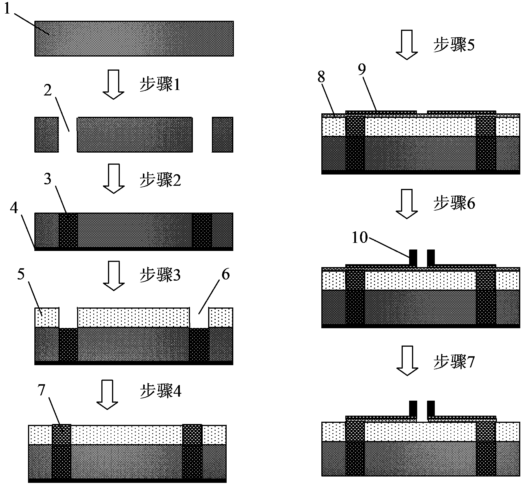
[0038] This embodiment provides a micro-electromechanical system probe card based on an elastic substrate and back leads and a preparation method. Using the method of back leads, the structural parameters of the prepared probe card are: ceramic substrate, substrate thickness 1mm, substrate Through-chip hole diameter 200μm, first metal seed layer thickness 200nm, polydimethylsiloxane elastic polymer layer thickness 150μm, elastic polymer through-hole structure diameter 200μm, second metal seed layer thickness 100nm, copper metal circuit layer thickness 5μm, line width 100μm, metal probe structure height 75μm.
[0039] Such as figure 1 Shown, the preparation method in this implementation comprises the following steps:
[0040] The first step is to punch through holes on the substrate;
[0041] A ceramic sheet with a thickness of 1 mm was used as the substrate, and a through-hole with a diameter of 200 μm was prepared by mechanical drilling; it was ultrasonically cleaned with d...
Embodiment 2
[0055] This embodiment provides a micro-electromechanical system probe card based on an elastic substrate and back leads and a preparation method. Using the method of back leads, the structural parameters of the prepared probe card are: PCB substrate, substrate thickness 2mm, substrate Diameter of through-chip hole is 100 μm, thickness of first metal seed layer is 100 nm, thickness of polydimethylsiloxane elastic polymer layer is 250 μm, diameter of elastic polymer via structure is 150 μm, thickness of second metal seed layer is 200 nm, thickness of copper metal circuit layer 10μm, line width 50μm, metal probe structure height 100μm.
[0056] Such as figure 1 Shown, the preparation method in this implementation comprises the following steps:
[0057] The first step is to punch through holes on the substrate;
[0058] A PCB with a thickness of 2mm is used as the substrate, and a through-hole with a diameter of 100 μm is prepared by laser hole method; it is ultrasonically clea...
Embodiment 3
[0072] This embodiment provides a MEMS probe card based on an elastic substrate and back leads and its preparation method. The probe card structure parameters prepared by using the back lead method are: silicon substrate, substrate thickness 500 μm, substrate The diameter of the via hole is 30 μm, the thickness of the first metal seed layer is 50 nm, the thickness of the polydimethylsiloxane elastic polymer layer is 40 μm, the diameter of the elastic polymer via structure is 30 μm, the thickness of the second metal seed layer is 20 nm, and the thickness of the copper metal circuit layer is 2 μm , the line width is 5 μm, and the height of the metal probe structure is 30 μm.
[0073] Such as figure 1 Shown, the preparation method in this implementation comprises the following steps:
[0074] The first step is to punch through holes on the substrate;
[0075] A silicon wafer with a thickness of 500 μm was used as the substrate, and through holes with a diameter of 30 μm were pr...
PUM
| Property | Measurement | Unit |
|---|---|---|
| Aperture | aaaaa | aaaaa |
| Thickness | aaaaa | aaaaa |
| Thickness | aaaaa | aaaaa |
Abstract
Description
Claims
Application Information
 - R&D
- Intellectual Property
- Life Sciences
- Materials
- Tech Scout
- Unparalleled Data Quality
- Higher Quality Content
- 60% Fewer Hallucinations
Browse by: Latest US Patents, China's latest patents, Technical Efficacy Thesaurus, Application Domain, Technology Topic, Popular Technical Reports.
© 2025 PatSnap. All rights reserved.Legal|Privacy policy|Modern Slavery Act Transparency Statement|Sitemap|About US| Contact US: help@patsnap.com