
Multi-layer nanometer composite thin film material for high-speed high-density phase transition storage and method for preparing material

A technology of phase change memory and thin film material, which is applied in the field of materials in the field of microelectronics technology, and can solve the problems that the phase change speed needs to be improved, and the requirements cannot be fully met.

Inactive Publication Date: 2013-10-30
TONGJI UNIV
View PDF3 Cites 11 Cited by
  • Summary
  • Abstract
  • Description
  • Claims
  • Application Information

AI Technical Summary

Problems solved by technology

Although there are not too many shortcomings, there are many places to be improved and improved (Seo, Jae-Hee, etc., Journal of Applied Physics, 108, 064515, 2010)
For example, Ge2Sb2Te5 film has only two resistance states, high and low, corresponding to logical "0" and "1" , there is room for improvement in storage density; secondly, the phase transition time of Ge2Sb2Te5 film is about 20ns, and It cannot fully meet the requirements of future high-speed storage, so its phase change speed needs to be improved

Method used


Image

  • Multi-layer nanometer composite thin film material for high-speed high-density phase transition storage and method for preparing material
  • Multi-layer nanometer composite thin film material for high-speed high-density phase transition storage and method for preparing material
  • Multi-layer nanometer composite thin film material for high-speed high-density phase transition storage and method for preparing material

Examples


Embodiment 1

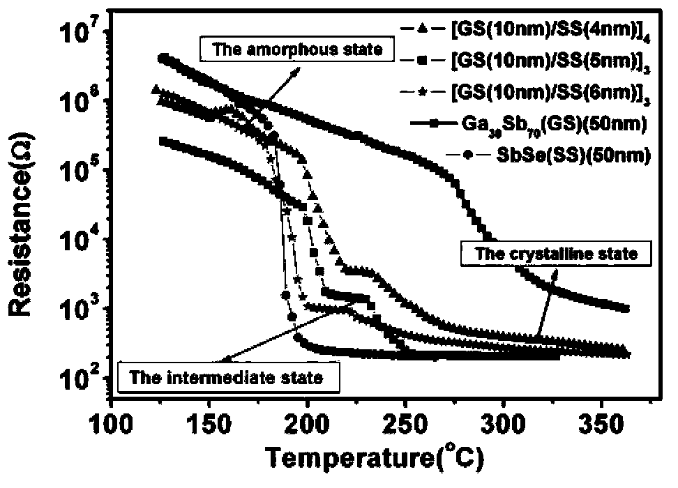
[0022] [SS (anm) / GS (bnm)] prepared in the present embodiment x The specific material structure is [SS(4nm) / GS(10nm)] 4 .

[0023] Its preparation steps are:

[0024] 1. Clean SiO2 2 / Si(100) substrate, cleaning the surface and back, removing dust particles, organic and inorganic impurities;

[0025] a) strong ultrasonic cleaning in acetone solution for 3-5 minutes, and rinse with deionized water;

[0026] b) Strong ultrasonic cleaning in ethanol solution for 3-5 minutes, rinse with deionized water, high-purity N 2 Blow dry the surface and back;

[0027] c) Dry the water vapor in an oven at 120°C for about 20 minutes.

[0028] 2. Prepared by magnetron sputtering [SS(4nm) / GS(10nm)]4 Preparation before multilayer composite film:

[0029] a) Install SbSe and Ga 30 Sb 70 Sputtering target material, the purity of the target material reaches 99.999% (atomic percentage), and the background vacuum is evacuated to 1×10 -4 Pa;

[0030] b) Set the sputtering power to 20W;

[...

Embodiment 2

[0040] [SS(anm) / GS(bnm)] prepared in this example x The specific structures of nano phase change thin film materials are [SS(5nm) / GS(10nm)] 3 and [SS(6nm) / GS(10nm)] 3 , and the [SS(5nm) / GS(10nm)] 3 and [SS(6nm) / GS(10nm)] 3 The thickness of the multi-layer phase change thin film material is about 50nm.

[0041] Above [SS(5nm) / GS(10nm)] 3 and [SS(6nm) / GS(10nm)] 3 The preparation method of the multilayer composite phase change thin film material is the same as that of Example 1.


PUM

PropertyMeasurementUnit
thicknessaaaaaaaaaa
thicknessaaaaaaaaaa

Abstract

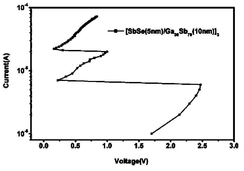
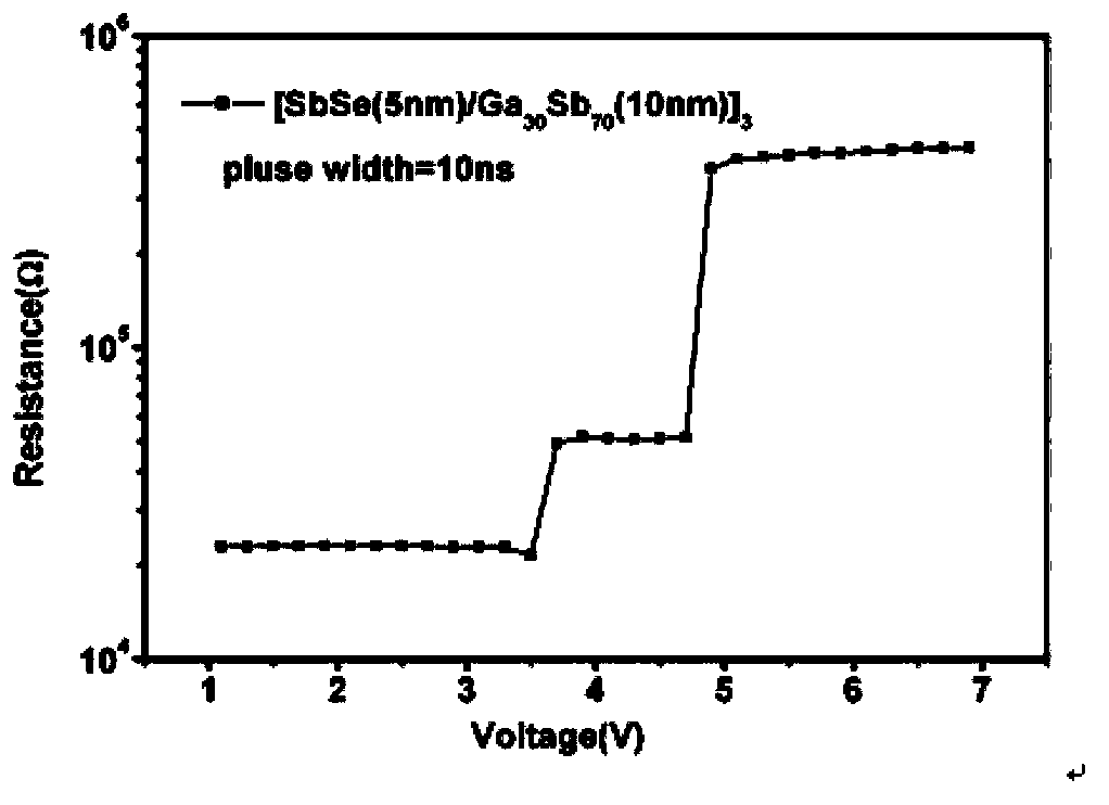
The invention discloses a multi-layer nanometer composite thin film material for a high-speed high-density phase transition storage. The multi-layer nanometer composite thin film material is a SbSe / Ga30Sb70 multi-layer composite thin film, and the structure of the multi-layer nanometer composite thin film material conforms to the following general formula: [SbSe (a) / Ga30Sb70 (b)]x, and is capable of being abbreviated to be [SS(a) / GS(b)]x. In the formula, the a and the b represent the thickness of a single-layer SbSe thin film and the thickness of a single-layer Ga30Sb70 thin film respectively, wherein the a conforms to the following formula: 1<=a<=50nm, the b conforms to the following formula: 1<=b<=50nm, the x represents the number of alternating cycles of the single-layer SbSe thin film and the single-layer Ga30Sb70 thin film or the number of alternating layers of the single-layer SbSe thin film and the single-layer Ga30Sb70 thin film, and the x is equal to 1 or 2 or 3 or 4. The SbSe / Ga30Sb70 multi-layer composite phase transition thin film is formed in a composite mode at the nanometer level, has a high resistance state, a middle resistance state and a low resistance state, is capable of achieving multi-stage storage, and greatly improves the storage density and the reading and writing operation speed of the storage.

Description

technical field [0001] The invention relates to a material in the technical field of microelectronics, in particular to a SbSe / Ga material used for high-speed and high-density phase-change memory 30 Sb 70 Multilayer nanocomposite film materials. Background technique [0002] Phase change memory (PCRAM) is a new type of non-volatile memory that uses material crystalline-amorphous state conversion to realize information storage. This kind of phase change material has low resistance in crystalline state and high resistance in amorphous state, and uses the difference between high and low resistance as different storage states for information storage. The Joule heat generated by electric pulses is used to realize the repeated conversion between the high resistance state and the low resistance state, so as to achieve the purpose of information storage. It has the advantages of high storage density, low power consumption, fast reading speed, strong stability, and compatibility w...

Claims


Application Information

Patent Timeline
Patent Type & Authority Applications(China)
IPC IPC(8): H01L45/00B82Y30/00
Inventor 翟继卫胡益丰
Owner TONGJI UNIV
Learn More