
Method for passivating amorphous silicon and polycrystalline silicon film interfaces and manufacturing single junction polycrystalline silicon amorphous silicon (SPA) structure heterojunction with intrinsic thin-layer (HIT) cell

A technology of polysilicon thin film and amorphous silicon, which is applied in the field of solar cells, can solve the problem of many defect states, achieve the effects of reducing recombination, reducing interface state density, and improving conversion efficiency

Inactive Publication Date: 2013-08-21
INST OF SEMICONDUCTORS - CHINESE ACAD OF SCI
View PDF7 Cites 7 Cited by
  • Summary
  • Abstract
  • Description
  • Claims
  • Application Information

AI Technical Summary

Problems solved by technology

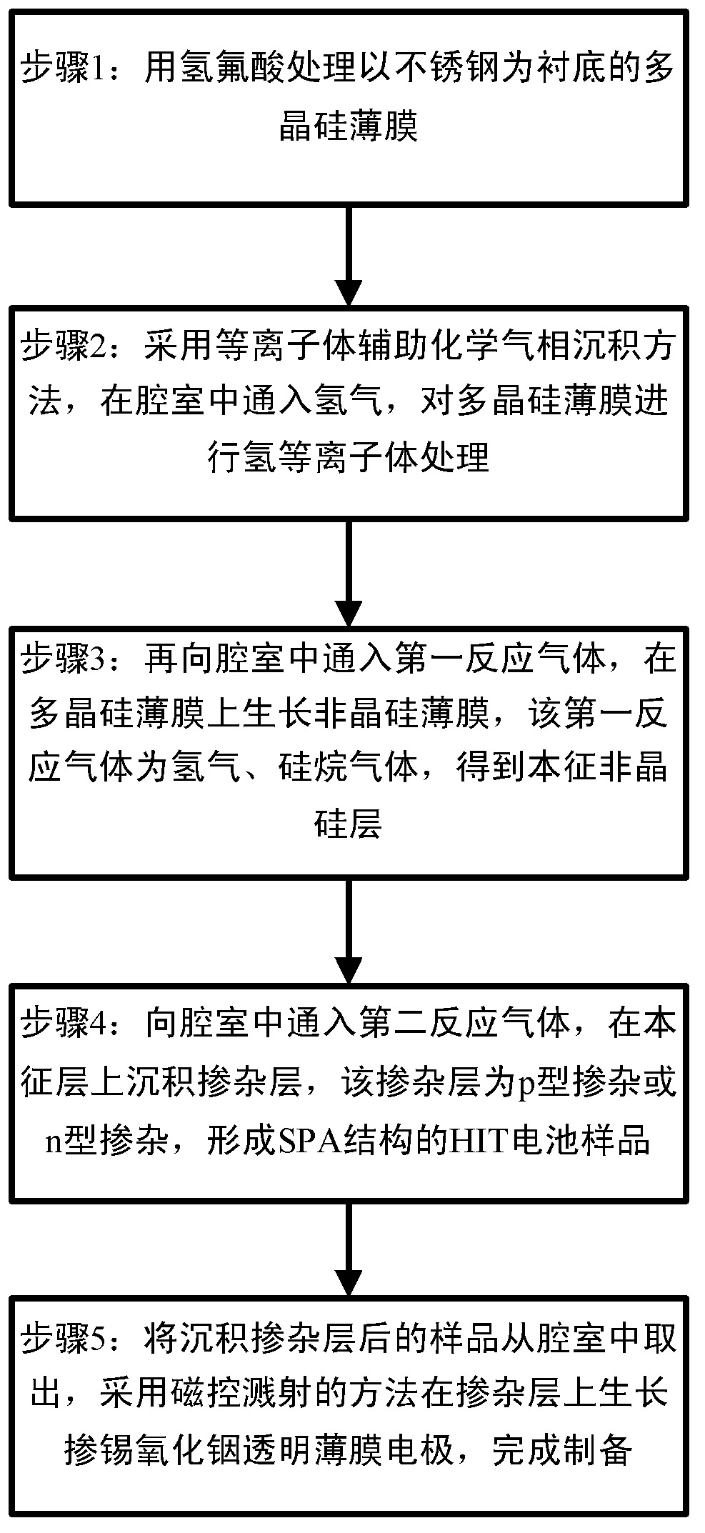
[0007] In order to overcome the problem of many defect states at the interface between amorphous silicon and polysilicon film, the present invention provides a passivation method for the interface between amorphous silicon and polysilicon film in solar cells and the application of the method to prepare n-type polysilicon film SPA structure HIT battery method

Method used


Image

  • Method for passivating amorphous silicon and polycrystalline silicon film interfaces and manufacturing single junction polycrystalline silicon amorphous silicon (SPA) structure heterojunction with intrinsic thin-layer (HIT) cell

Examples


Embodiment Construction

[0028] In order to make the object, technical solution and advantages of the present invention clearer, the present invention will be described in further detail below in conjunction with specific embodiments and with reference to the accompanying drawings.

[0029] The passivation method of solar cell amorphous silicon and polysilicon film interface provided by the present invention is to adopt plasma enhanced chemical vapor deposition (Plasma Enhanced Chemical Vapor Deposition, PECVD), under the situation of passing into chamber hydrogen, to solar cell The interface between amorphous silicon and polysilicon film is passivated. Wherein, the specific process of passivating the interface between the amorphous silicon and the polysilicon film of the solar cell is as follows: the polysilicon film sample to be treated is placed in a plasma-enhanced chemical vapor deposition device with a radio frequency of 13.56 MHz, and the Put hydrogen gas into the equipment, the flow rate of hy...


PUM

PropertyMeasurementUnit
thicknessaaaaaaaaaa
thicknessaaaaaaaaaa

Abstract

The invention discloses a method for passivating amorphous silicon and polycrystalline silicon film interfaces of a solar cell and a method for manufacturing an n-type polycrystalline silicon film single junction polycrystalline silicon amorphous silicon (SPA) structure heterojunction with intrinsic thin-layer (HIT) cell through the method. The method for passivating the amorphous silicon and polycrystalline silicon film interfaces of the solar cell comprises the steps of strengthening chemical vapor depositions through plasma, and carrying out passivation processing on the amorphous silicon and polycrystalline silicon film interfaces of the solar cell under the condition that ammonia is led into a cavity. A surface state of a polycrystalline silicon film can be reduced through hydrogen plasma interface processing. Therefore, interface states of amorphous silicon and polycrystalline silicon films of the SPA structure HIT cell are reduced, synthesis of photon-generated carriers generated under illumination at the positions of the interfaces is reduced, collection of the photo-generated carriers is increased, and conversion efficiency of the cell is improved.

Description

technical field [0001] The invention relates to the technical field of solar cells, in particular to a heterojunction with intrinsic layer (Heterojunction with Intrinsic Thin-Layer, HIT) solar cell with a single junction polycrystalline silicon amorphous silicon (SPA) structure A method for passivating the interface between battery amorphous silicon and polysilicon film and a method for preparing HIT battery with n-type polysilicon film SPA structure using the method. Background technique [0002] Among the current solar cells, silicon thin-film cells are highly valued for their advantages of non-toxicity, abundant raw materials, and low cost. However, in the process of studying silicon thin film batteries, it was found that the interface of silicon thin film batteries has a great influence on the collection of photogenerated carriers and thus the performance of the battery. If the interface is well processed, the density of states at the interface is lower, the collection ...

Claims


Application Information

Patent Timeline
Patent Type & Authority Applications(China)
IPC IPC(8): H01L31/20
CPCY02P70/50
Inventor 李浩曾湘波谢小兵杨萍李敬彦张晓东王启明
Owner INST OF SEMICONDUCTORS - CHINESE ACAD OF SCI
Learn More