Silicon carbide semiconductor device and method for manufacturing same

a semiconductor device and silicon carbide technology, applied in the direction of semiconductor devices, basic electric elements, electrical equipment, etc., can solve the problem of leakage current likely to flow between the first and second electrodes

Active Publication Date: 2013-04-25
SUMITOMO ELECTRIC IND LTD
View PDF0 Cites 17 Cited by
  • Summary
  • Abstract
  • Description
  • Claims
  • Application Information

AI Technical Summary

Benefits of technology

This patent relates to a method for improving the performance of silicon carbide semiconductor devices. The method includes steps to enhance carrier mobility and reduce channel resistance by forming a channel surface with a specific orientation. The channel surface can be created by forming a trench with an inner wall including the channel surface. The method also includes using a process gas containing a halogen element to spontaneously form a surface corresponding to the desired orientation. By doing so, a smaller on-resistance can be achieved, resulting in a more efficient semiconductor device. Additionally, the method includes providing a low interface state density between the insulating film and the side wall and bottom surface of the substrate, which can suppress current leakage between the electrodes. Overall, this patent presents a technical solution to improve the performance and efficiency of silicon carbide semiconductor devices.

Problems solved by technology

As a result of inspection by the present inventors, it has been found that when a crystallographical plane orientation of the silicon carbide substrate is inappropriate in the termination region, interface state density becomes high in the interface between the silicon carbide substrate and the insulating film, with the result that leakage current is likely to flow between the first and second electrodes.

Method used


Image

  • Silicon carbide semiconductor device and method for manufacturing same
  • Silicon carbide semiconductor device and method for manufacturing same
  • Silicon carbide semiconductor device and method for manufacturing same

Examples


Embodiment Construction

[0022]The following describes an embodiment of the present invention with reference to figures. It should be noted that in the below-mentioned figures, the same or corresponding portions are given the same reference characters and are not described repeatedly. Regarding crystallographic indications in the present specification, an individual plane is represented by ( ) and a group plane is represented by { }. To indicate a negative index of a plane, a negative symbol is put before a numeral instead of putting “-” (bar) above the numeral. For description of an angle, a system in which an omnidirectional angle is 360° is employed.

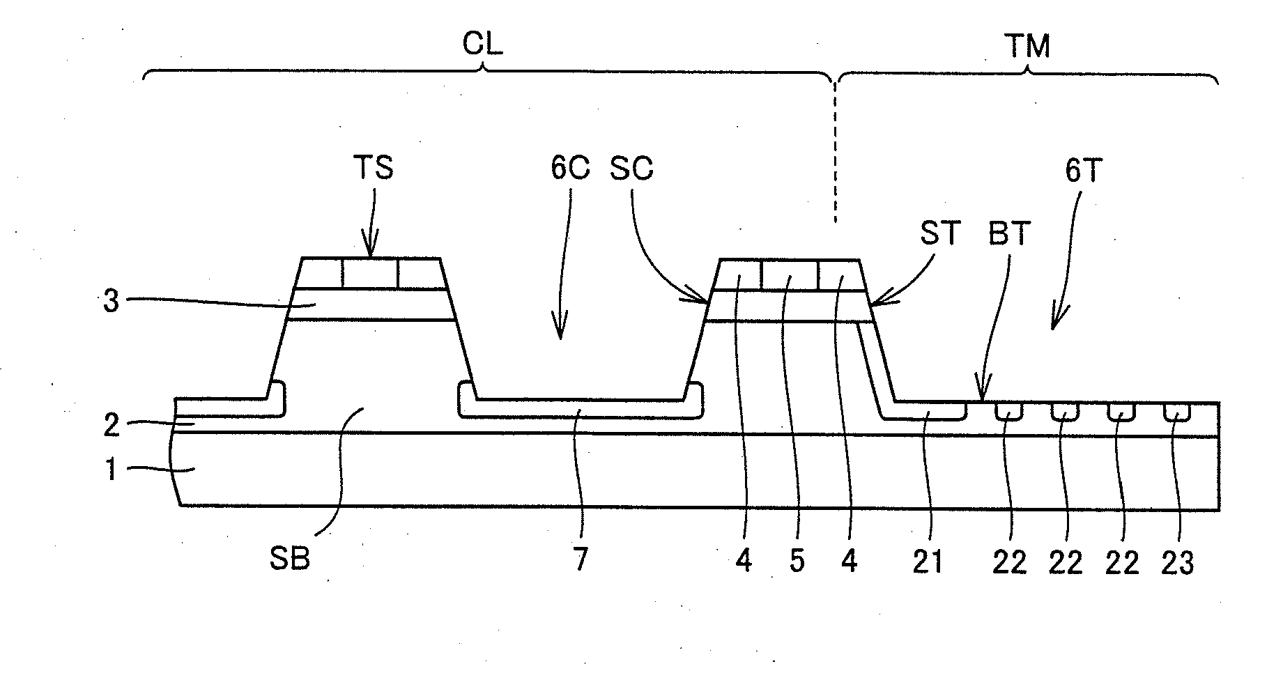
[0023]First, the following describes a gist of a configuration of a MOSFET serving as a silicon carbide semiconductor device of the present embodiment.

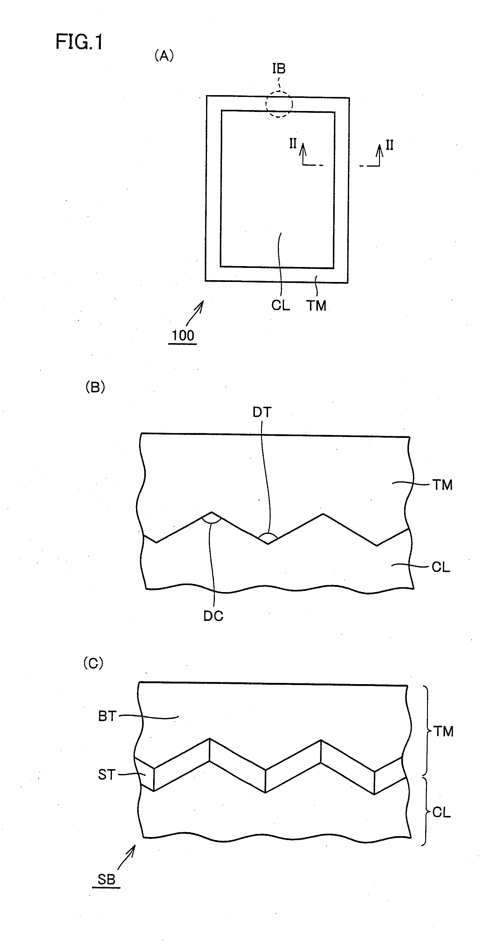
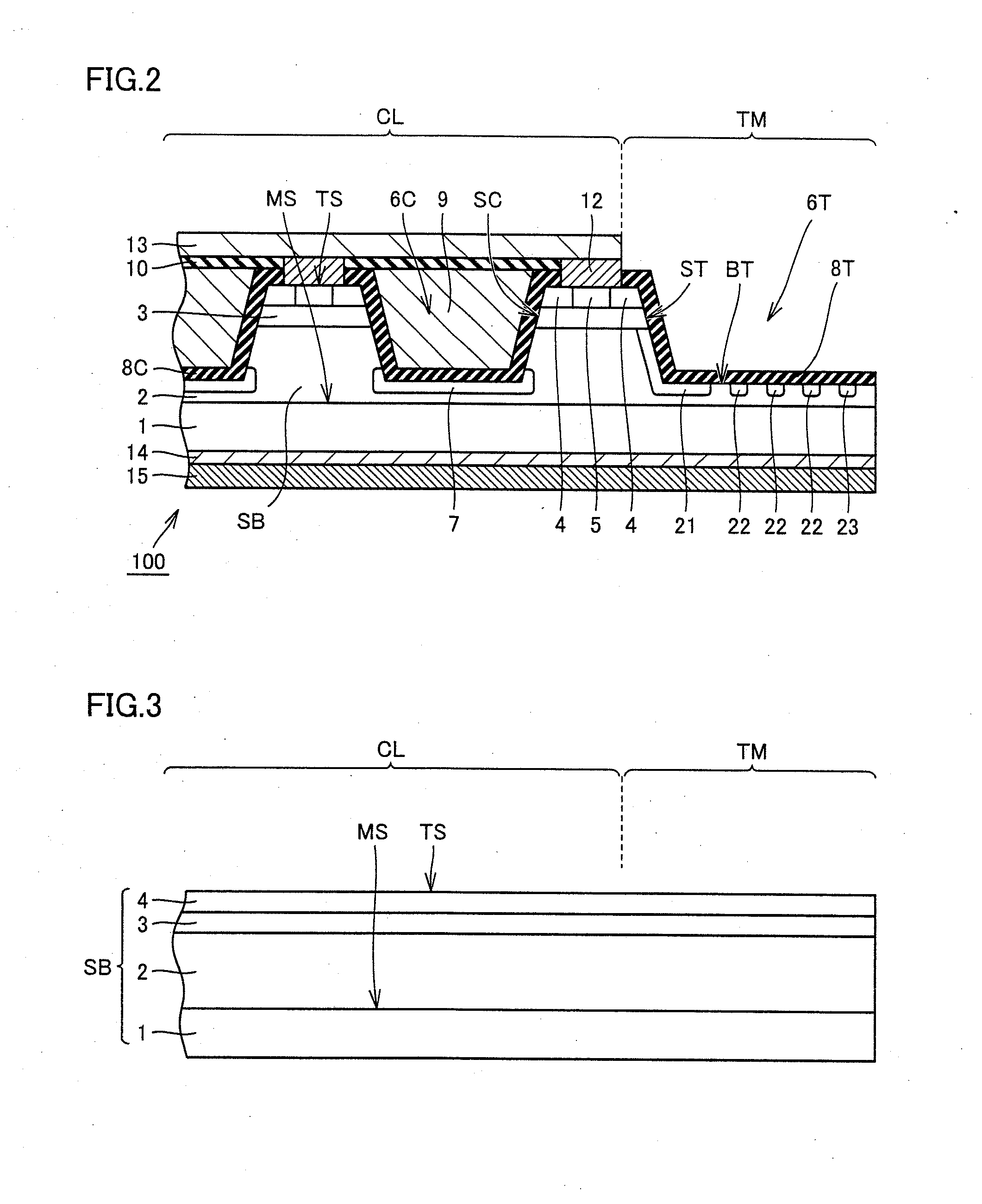
[0024]As shown in FIG. 1(A), when viewed in a plan view, MOSFET 100 has an element region CL provided with a transistor element (semiconductor element), and a termination region TM surrounding element region CL...


PUM

PropertyMeasurementUnit
angleaaaaaaaaaa
angle DCaaaaaaaaaa
off angleaaaaaaaaaa

Abstract

When viewed in a plan view, a termination region (TM) surrounds an element region (CL). A first side of a silicon carbide substrate (SB) is thermally etched to form a side wall (ST) and a bottom surface (BT) in the silicon carbide substrate (SB) at the termination region (TM). The side wall (ST) has a plane orientation of one of {0-33-8} and {0-11-4}. The bottom surface (BT) has a plane orientation of {000-1}. On the side wall (ST) and the bottom surface (BT), an insulating film (8T) is formed. A first electrode (12) is formed on the first side of the silicon carbide substrate (SB) at the element region (CL). A second electrode (14) is formed on a second side of the silicon carbide substrate (SB).

Description

BACKGROUND OF THE INVENTION[0001]1. Field of the Invention[0002]The present invention relates to a silicon carbide semiconductor device and a method for manufacturing the silicon carbide semiconductor device, more particularly, a silicon carbide semiconductor device having an element region provided with a semiconductor element and a termination region surrounding the element region when viewed in a plan view, as well as a method for manufacturing such a silicon carbide semiconductor device.[0003]2. Description of the Background Art[0004]According to Japanese Patent Laying-Open No. 2010-147222 (Patent Literature 1), a SiC semiconductor device has a cell region provided with a MOSFET and an outer circumferential region surrounding the cell region. In the outer circumferential region, a mesa structure portion constructed by a recess is formed. At a boundary portion between the cell region and the outer circumferential region, a p type resurf layer is formed to surround the outer circu...

Claims


Application Information

Patent Timeline
Patent Type & Authority Applications(United States)
IPC IPC(8): H01L29/161H01L21/336
CPCH01L29/4236H01L29/66068H01L29/7811H01L29/7813H01L29/045H01L29/1608H01L29/0619H01L29/0623H01L29/0638H01L29/0657H01L29/0661H01L29/0615H01L21/3065
Inventor HIYOSHI, TORUMASUDA, TAKEYOSHIWADA, KEIJI
Owner SUMITOMO ELECTRIC IND LTD
Why Eureka
Try Eureka