Reverse polymer solar cell with dual electron transport layer structure
A dual-electron transmission, solar cell technology, applied in circuits, photovoltaic power generation, electrical components, etc., can solve problems such as low power consumption, high photogenerated electron collection efficiency, and high performance
- Summary
- Abstract
- Description
- Claims
- Application Information
AI Technical Summary
Problems solved by technology
Method used
Image
Examples
Embodiment 1
[0055] Prepare the structure as ITO with a thickness of 100nm / PMMA with a thickness of 10nm:C 60 :LCV=1:20:2 / Amorphous TiO with a thickness of 10nm 2 / P3HT:PC with a thickness of 80nm 61 BM=12:10 / MoO with a thickness of 10nm 3 A reverse polymer solar cell with a double electron transport layer structure of Al with a thickness of 100nm.
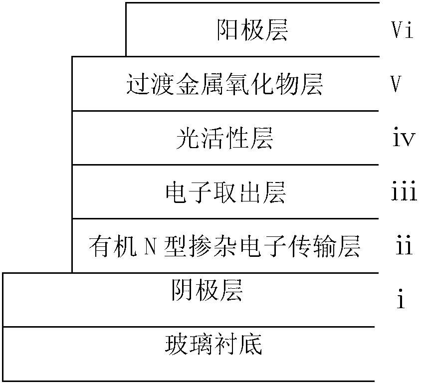
[0056] The reverse polymer solar cell with double electron transport layer structure is composed of a layer of ITO cathode layer with a thickness of 100nm on a glass substrate, a layer of PMMA with a thickness of 10nm deposited on the ITO cathode layer:C 60 : LCV thin film organic N-type doped electron transport layer, one layer deposited on PMMA:C 60 : Amorphous TiO with a thickness of 10nm on the organic N-type doped electron transport layer of LCV thin film 2 Thin-film electron extraction layer, a layer deposited on amorphous TiO 2 P3HT:PC with a thickness of 80nm on the thin film electron extraction layer 61 BM film photoactive layer...
Embodiment 2
[0083] The preparation structure is ITO with a thickness of 100nm / PMMA with a thickness of 20nm:C 60 :LCV=1:5:0.1 / Amorphous ZnO with a thickness of 10nm / PCPDTBT:PC with a thickness of 150nm 71 BM=12:10 / MoO with a thickness of 10nm 3 A reverse polymer solar cell with a double electron transport layer structure of Al with a thickness of 100nm.
[0084] The reverse polymer solar cell with double electron transport layer structure is composed of a layer of ITO cathode layer with a thickness of 100nm on a glass substrate, a layer of PMMA with a thickness of 20nm deposited on the ITO cathode layer:C 60 : LCV thin film organic N-type doped electron transport layer, one layer deposited on PMMA:C 60 : An amorphous ZnO thin film electron extraction layer with a thickness of 10nm on the organic N-type doped electron transport layer of the LCV film, a layer of PCPDTBT with a thickness of 150nm deposited on the amorphous ZnO thin film electron extraction layer:PC 71 BM film photoactive ...
Embodiment 3
[0102] The preparation structure is Ag / PMMA with a thickness of 20nm / thickness of 10nm:C 60 :AOB=1:20:2 / Amorphous ZnO with a thickness of 10nm / P3HT with a thickness of 80nm:PC 61 BM=12:10 / MoO with a thickness of 10nm 3 A reverse polymer solar cell with a double electron transport layer structure of Al with a thickness of 100nm.
[0103] The reverse polymer solar cell with double electron transport layer structure is composed of a layer of Ag ITO cathode layer with a thickness of 20nm on a glass substrate, and a layer of PMMA:C with a thickness of 10nm deposited on the ITO cathode layer. 60 :AOB thin film organic N-type doped electron transport layer, one layer deposited on PMMA:C 60:Amorphous ZnO thin film electron extraction layer with a thickness of 10nm on the organic N-type doped electron transport layer of AOB film, a layer of P3HT:PC with a thickness of 80nm deposited on the amorphous ZnO thin film electron extraction layer 61 BM film photoactive layer, a layer deposi...
PUM
 Abstract
Description
Claims
Application Information
 - R&D
- Intellectual Property
- Life Sciences
- Materials
- Tech Scout
- Unparalleled Data Quality
- Higher Quality Content
- 60% Fewer Hallucinations
Browse by: Latest US Patents, China's latest patents, Technical Efficacy Thesaurus, Application Domain, Technology Topic, Popular Technical Reports.
© 2025 PatSnap. All rights reserved.Legal|Privacy policy|Modern Slavery Act Transparency Statement|Sitemap|About US| Contact US: help@patsnap.com


