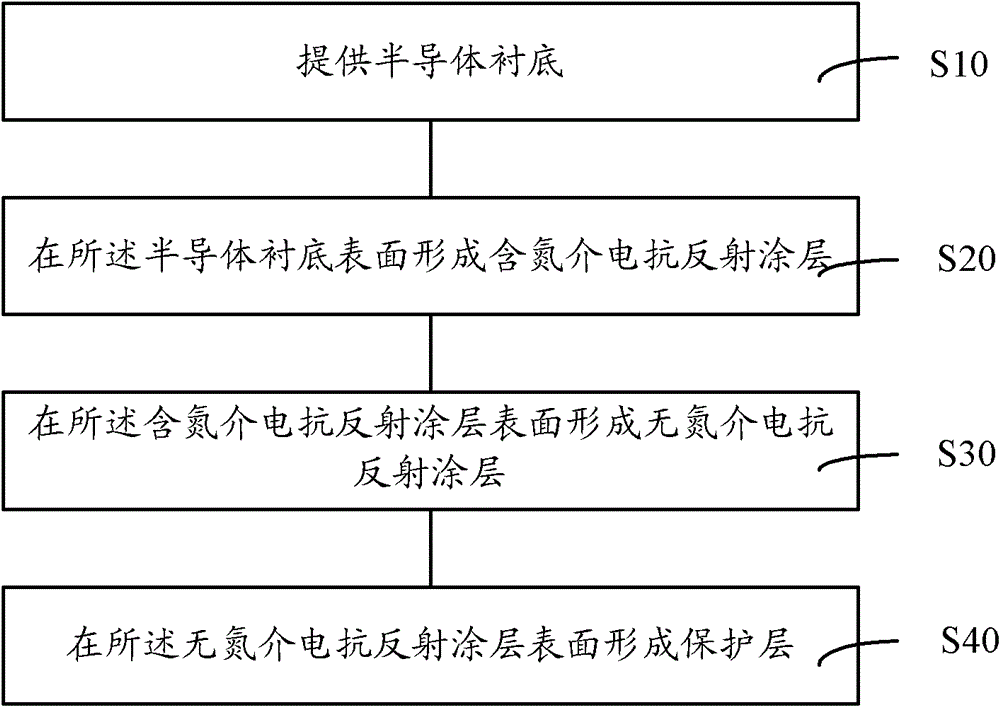
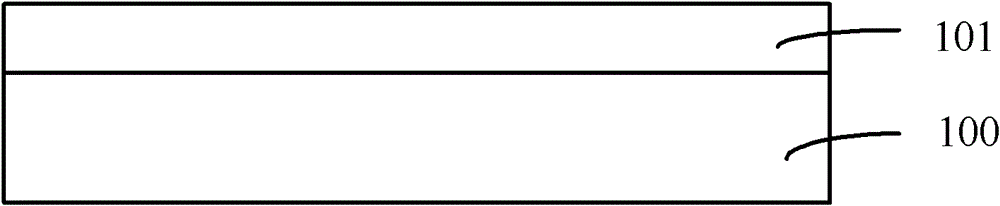
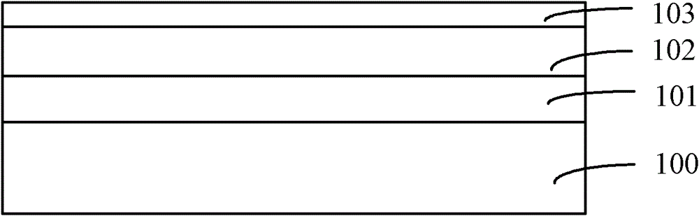
Method for forming dielectric anti-reflection coating and photolithography method
An anti-reflection coating and dielectric technology, which is used in the manufacture of circuits, electrical components, semiconductor/solid-state devices, etc., can solve the problems of small modulation range, difficult to control optical performance, and can not meet the needs of the process, and achieve convenient modulation process. Effect
- Summary
- Abstract
- Description
- Claims
- Application Information
AI Technical Summary
Problems solved by technology
Method used
Image

Examples
Embodiment Construction
[0043] The existing nitrogen-free dielectric anti-reflective coating (NFDARC) usually adopts plasma enhanced chemical vapor deposition (PECVD), and the gas used is SiH 4 and CO 2 , when forming a nitrogen-free dielectric antireflection coating, by controlling the SiH 4 and CO 2 flow rate to adjust the extinction coefficient (K) and refractive index (N) of the nitrogen-free dielectric anti-reflective coating. In the actual production process, there are differences in the wavelength of the semiconductor substrate, photoresist material, and exposure light source. In order to obtain better photoresist exposure morphology, it is necessary to form a nitrogen-free dielectric anti-reflective coating (NFDARC) with different extinction coefficients (K) and refractive indices (N). The inventors found that the existing method forms The modulation range of the extinction coefficient (K) and the refractive index (N) of the nitrogen-free dielectric antireflection coating is small, and the ...
PUM
| Property | Measurement | Unit |
|---|---|---|
| thickness | aaaaa | aaaaa |
| thickness | aaaaa | aaaaa |
Abstract
Description
Claims
Application Information
 - R&D
- Intellectual Property
- Life Sciences
- Materials
- Tech Scout
- Unparalleled Data Quality
- Higher Quality Content
- 60% Fewer Hallucinations
Browse by: Latest US Patents, China's latest patents, Technical Efficacy Thesaurus, Application Domain, Technology Topic, Popular Technical Reports.
© 2025 PatSnap. All rights reserved.Legal|Privacy policy|Modern Slavery Act Transparency Statement|Sitemap|About US| Contact US: help@patsnap.com