Variable capacitor and differential variable capacitor
A capacitor and differential technology, applied in the direction of circuits, electrical components, semiconductor devices, etc., can solve the problem of insufficient modulation range and achieve the effect of quality factor improvement and large modulation range
- Summary
- Abstract
- Description
- Claims
- Application Information
AI Technical Summary
Problems solved by technology
Method used
Image

Examples
no. 1 example
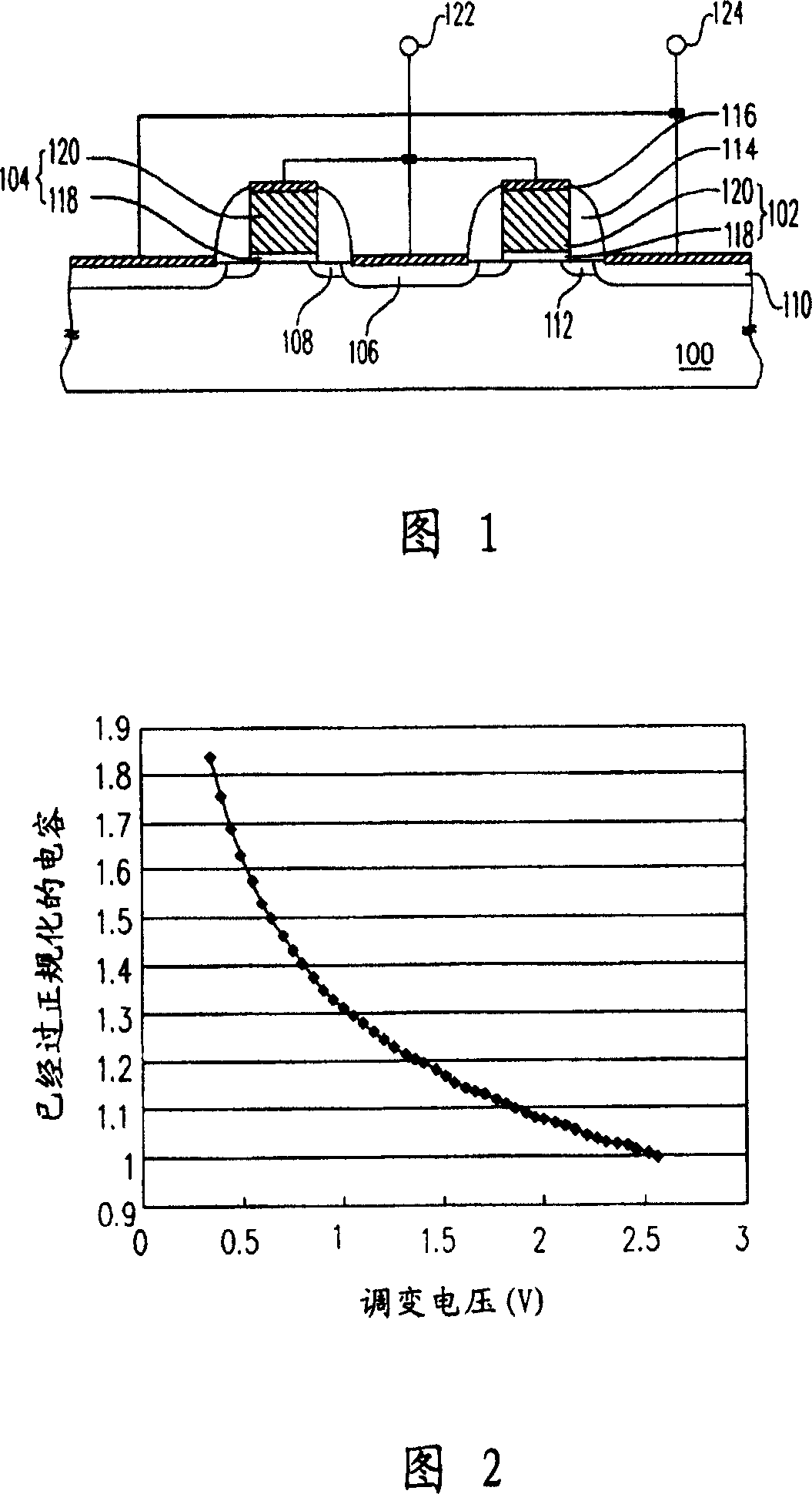
[0033] As shown in FIG. 1 , it shows a schematic cross-sectional view of a variable capacitor according to a preferred embodiment of the present invention. Referring to FIG. 1 , the variable capacitor of the present invention includes an n-type substrate 100 , two gate structures 102 , 104 , a p-type doped region 106 and an n-type doped region 110 . In a preferred embodiment, the variable capacitor further includes a p-type lightly doped region 108 , an n-type lightly doped region 112 , a spacer 114 and a metal silicide layer 116 .
[0034] The two gate structures 102 and 104 are disposed on the n-type substrate 100 , and each gate structure 102 and 104 is composed of a lower gate dielectric layer 118 and an upper gate conductive layer 120 . Moreover, the two gate structures 102 and 104 may also be disposed on a p-type substrate (not shown) having an n-type well region (not shown) in addition to being disposed on the n-type substrate 100 . In addition, the material of the gat...
no. 2 example
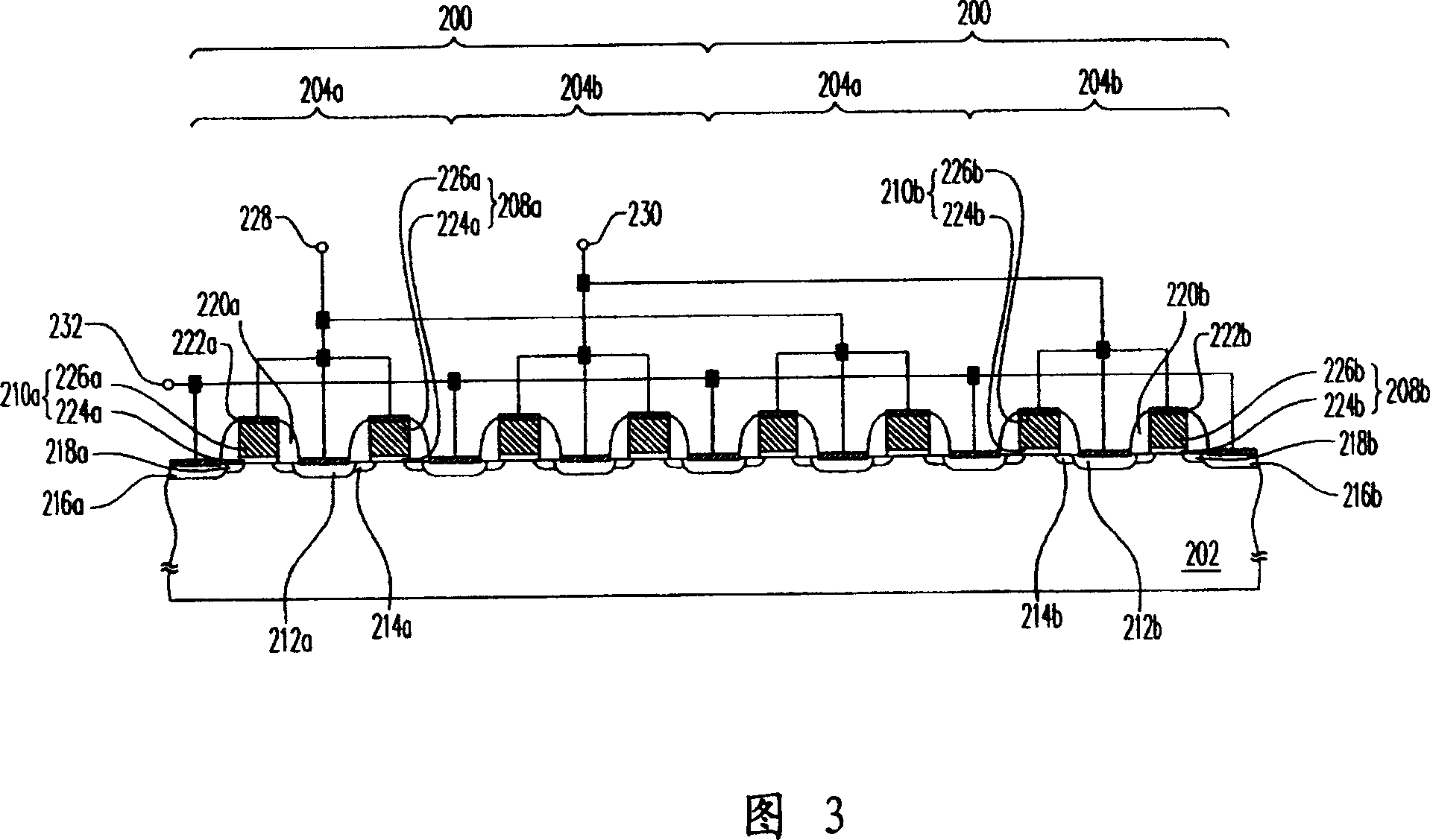
[0044] As shown in FIG. 3 , it shows a schematic cross-sectional view of a differential variable capacitor according to a preferred embodiment of the present invention, which is a variation application of the single variable capacitor of the first embodiment. Referring to FIG. 3, the differential variable capacitor of the present invention is composed of at least one pair of variable capacitors 200 disposed on an n-type substrate 202, and each pair of variable capacitors 200 includes a variable capacitor 204a and a variable capacitor 204a. Capacitor 204b.
[0045] Wherein, the variable capacitor 204a includes two gate structures 208a, 210a, a p-type doped region 212a and an n-type doped region 216a. In a preferred embodiment, the variable capacitor 204a further includes a p-type lightly doped region 214a, an n-type lightly doped region 218a, a spacer 220a and a metal silicide layer 222a.
[0046] The two gate structures 208a and 210a are disposed on the n-type substrate 202, ...
PUM
 Abstract
Description
Claims
Application Information
 - R&D
- Intellectual Property
- Life Sciences
- Materials
- Tech Scout
- Unparalleled Data Quality
- Higher Quality Content
- 60% Fewer Hallucinations
Browse by: Latest US Patents, China's latest patents, Technical Efficacy Thesaurus, Application Domain, Technology Topic, Popular Technical Reports.
© 2025 PatSnap. All rights reserved.Legal|Privacy policy|Modern Slavery Act Transparency Statement|Sitemap|About US| Contact US: help@patsnap.com