Multi-layer co-sintered lamination stackable chip resistor and manufacturing method thereof

A chip resistor, stacking technology, used in resistor manufacturing, resistors, trimmer resistors, etc., can solve the problems of efficient use, complicated locking and multi-layer co-firing, saving time and eliminating stacking procedures. Effect

Inactive Publication Date: 2013-05-29
PROSPERITY DIELECTRICS
View PDF3 Cites 0 Cited by
  • Summary
  • Abstract
  • Description
  • Claims
  • Application Information

AI Technical Summary

Problems solved by technology

[0005] However, the above-mentioned manufacturing method for making resistors is arranged for general single-layer resistors, and the same method for making stacked resistors is just to repeat the same method to extend its functionality. The process is not only complicated and locks Broken and did not make the most efficient use of the multi-layer co-firing technology

Method used


Image

  • Multi-layer co-sintered lamination stackable chip resistor and manufacturing method thereof
  • Multi-layer co-sintered lamination stackable chip resistor and manufacturing method thereof
  • Multi-layer co-sintered lamination stackable chip resistor and manufacturing method thereof

Examples


Embodiment Construction

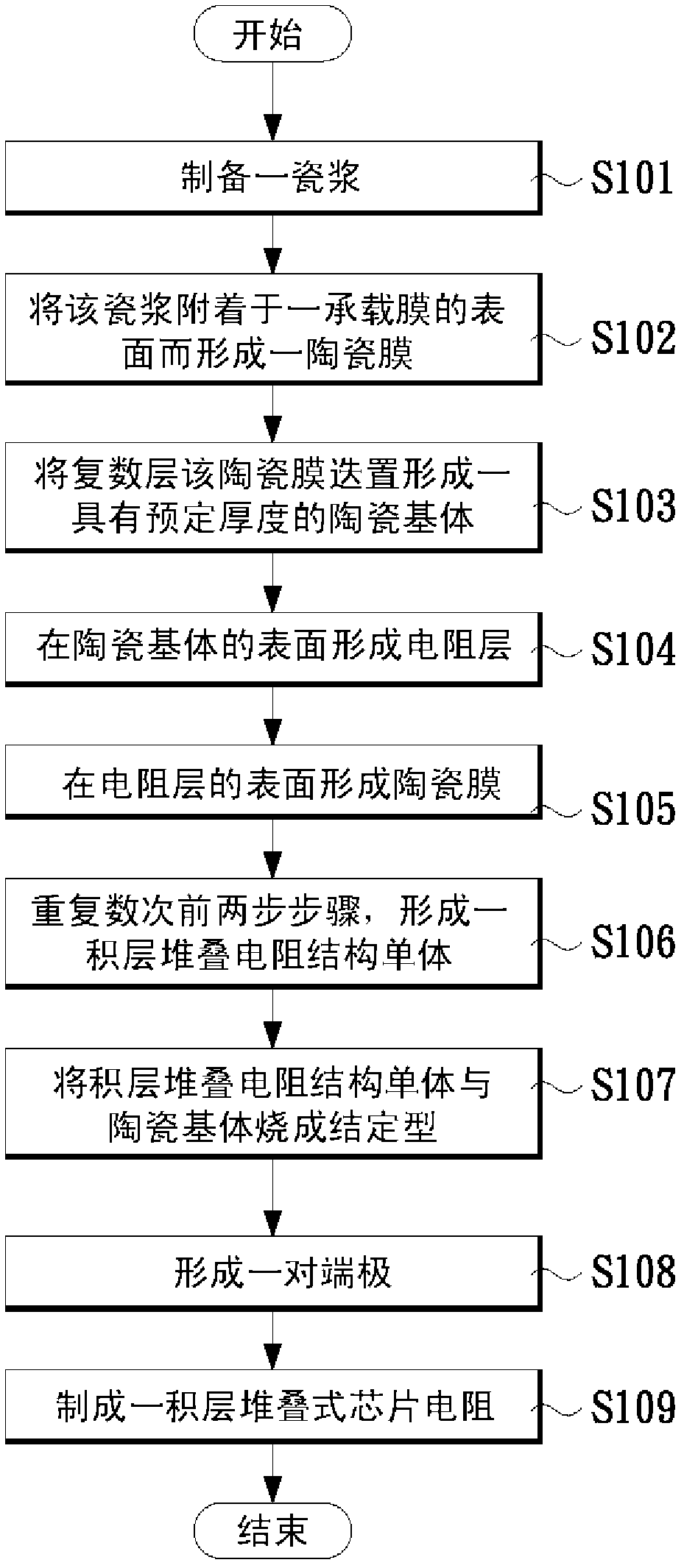
[0055] The multilayer co-fired multilayer stacked chip resistor and its manufacturing method provided by the present invention realize a multilayer stacked chip resistor structure by the multilayer cofiring technology.

[0056] The technical means adopted by the present invention to solve the problems of the known technologies is to firstly prepare a porcelain slurry including a solvent, a binder and a dispersant, and attach the porcelain slurry to the surface of a carrier film to form a ceramic film, and then A plurality of layers of the ceramic film are laminated to form a ceramic matrix with a predetermined thickness. Then a resistance layer is formed on the surface of the ceramic substrate, the ends of the resistance layer extend in a horizontal direction respectively to form terminal connection ends, and the ceramic film is formed on the surface of the resistance layer.

[0057] repeating the first two steps several times to form a monolithic stacked resistance structure ...


PUM


Abstract

The invention relates to a multi-layer co-sintered lamination stackable chip resistor and a manufacturing method of the multi-layer co-sintered lamination stackable chip resistor. The multi-layer co-sintered lamination stackable chip resistor comprises a ceramic substrate, a lamination stackable resistor structure body, a first terminal pole and a second terminal pole, wherein the ceramic substrate has a predetermined thickness and is formed by superposing a plurality of layers of ceramic membranes and attaching ceramic slurry containing a solvent, an adhesive and a dispersant to the surface of a bearing membrane, the lamination stackable resistor structure body is superposed on the ceramic substrate and comprises a plurality of layers of bearing membranes and a plurality of layers of resistive layers which are formed on the surfaces of the bearing membranes one by one, the resistive layers are parallel to one another and superposed in the vertical direction to separate a predetermined spacing, and the lamination stackable resistor structure body and the ceramic substrate are superposed and then sintered in a kiln at a predetermined sintering temperature and sintering time to finalize the design of the lamination stackable resistor structure body and the ceramic substrate by sintering.

Description

technical field [0001] The invention relates to a chip resistor, in particular to a multi-layer co-fired stacked chip resistor and a manufacturing method thereof. Background technique [0002] In the past, due to the factors of cost and characteristics, passive components could not be fully integrated into the integrated circuit, but had to be realized by means of external connection, which easily caused disadvantages such as low reliability, high production cost and difficulty in shrinking the substrate area, so there appeared The technology of multi-layer co-firing is used to solve the above-mentioned problems. Its connotation is mainly based on an oxide material in a high-temperature, oxygen-containing manufacturing environment, on the oxide ceramic layer made of insulating ceramic materials, using oxide electrodes instead of metal electrodes to prepare laminated or single-layer oxide ceramic components . [0003] The multi-layer co-firing technology not only makes the ...

Claims


Application Information

Patent Timeline
IPC IPC(8): H01C7/18H01C17/00H01C17/22
Inventor 巫宏俊周东毅蔡景仁蔡永承
Owner PROSPERITY DIELECTRICS
Why Eureka
Try Eureka