
Back-incidence solar cells with ingan/gan multilayer quantum well structure with variable in composition

A technology of solar cells and multi-layer quantum wells, applied in circuits, photovoltaic power generation, electrical components, etc., can solve the problems of the decrease of the critical thickness of the InGaN layer, the loss of short-circuit current, the serious recombination of photogenerated carriers, and the increase of the effective light absorption area. , the effect of reducing short-circuit current loss and improving conversion efficiency

Active Publication Date: 2016-09-14
INST OF SEMICONDUCTORS - CHINESE ACAD OF SCI
View PDF5 Cites 0 Cited by
  • Summary
  • Abstract
  • Description
  • Claims
  • Application Information

AI Technical Summary

Problems solved by technology

[0004] The absorption coefficient of the InGaN alloy near the band edge is as high as 105cm-1, which makes the InGaN absorbing layer absorb most of the incident light in the range of hundreds of nanometers. However, due to the lattice mismatch between InN and GaN of 11%, In The critical thickness of the InGaN material with a composition of 20% is only 10.7nm, increasing the In composition, the critical thickness of the InGaN layer will drop sharply
Therefore, for traditional p-i-n type InGaN solar cells, in order to obtain an InGaN absorber layer with better crystal quality, the highest In composition is only 12%-15%, and the conversion efficiency of the cell is less than 1%.
[0005] Solar cells generally adopt the normal incidence mode, and the light passes through the P-type layer and enters the quantum well absorption layer. Since the P and N electrodes are both on the front of the cell in the horizontal structure, the effective light-absorbing area of ​​the solar cell is reduced and the short-circuit current is lost.
At the same time, due to the limitations of P-GaN material growth technology, it is difficult to grow high-quality P-GaN materials, and the recombination of photogenerated carriers in P-GaN is serious, which affects the collection efficiency of carriers and is also a reason for the loss of short-circuit current. The back-incidence method will solve the above problems

Method used


Image

  • Back-incidence solar cells with ingan/gan multilayer quantum well structure with variable in composition
  • Back-incidence solar cells with ingan/gan multilayer quantum well structure with variable in composition

Examples


Embodiment Construction

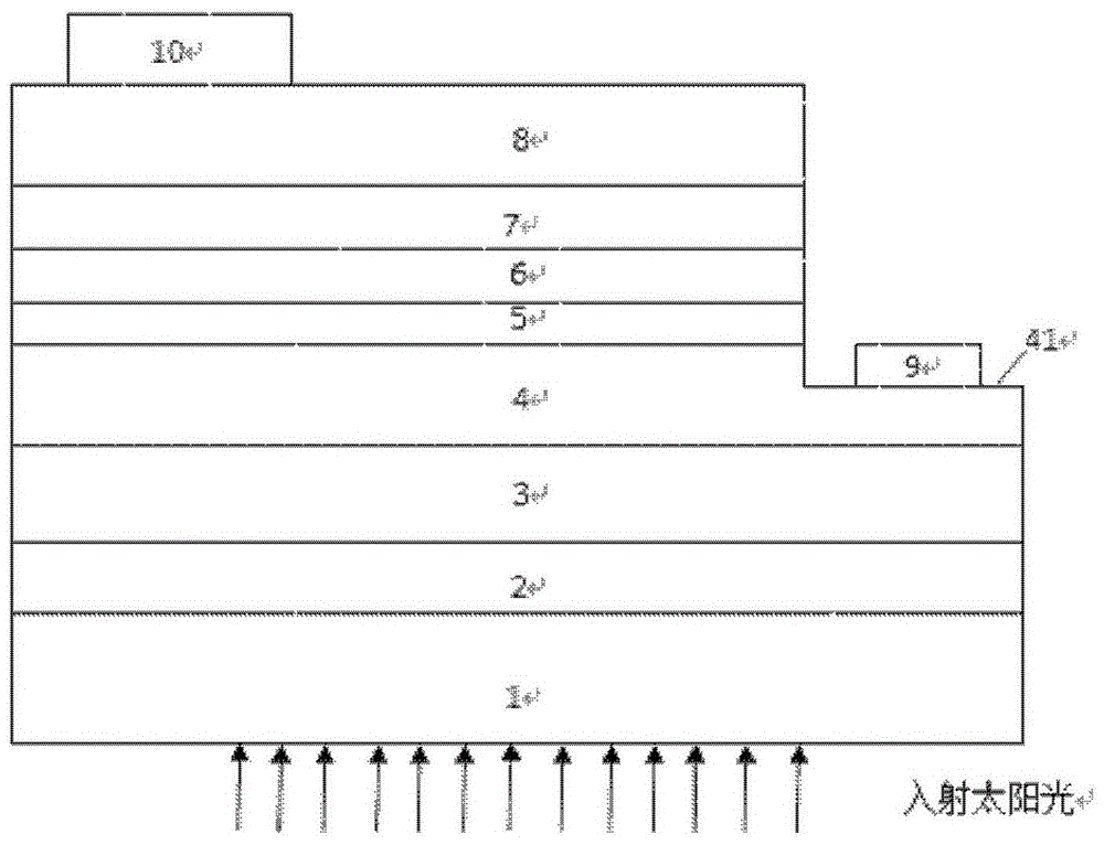
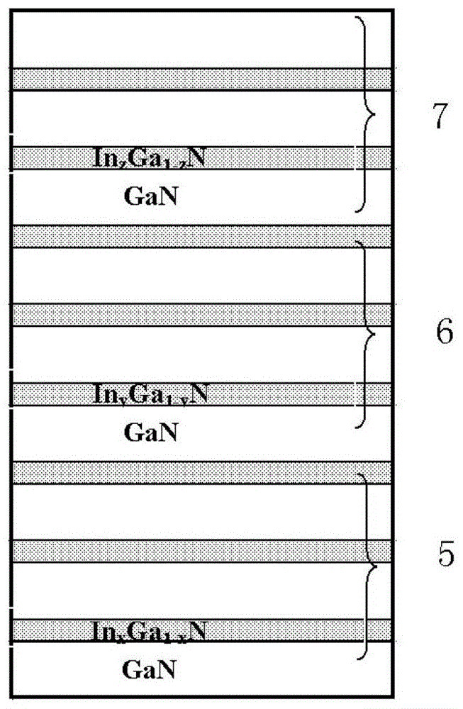
[0023] see figure 1 and figure 2 As shown, the present invention provides a kind of back-incidence solar cell containing variable In composition InGaN / GaN multilayer quantum well structure, which comprises:

[0024] A substrate 1, the substrate 1 is a double-sided polished sapphire or gallium nitride material, and the double-sided polished sapphire or gallium nitride substrate can reduce the incident light loss due to scattering during back incidence;

[0025] A low-temperature gallium nitride nucleation layer 2, the low-temperature gallium nitride nucleation layer is fabricated on the substrate 1, its growth temperature is 500°C-600°C, and its thickness is 0.2μm-0.3μm, the low-temperature gallium nitride formation The core layer 2 provides a nucleation center for the subsequent growth of gallium nitride material;

[0026] An unintentionally doped gallium nitride buffer layer 3, the unintentionally doped gallium nitride buffer layer 3 is fabricated on the low-temperature ga...


PUM


Abstract

A solar cell containing variable In component InGaN / GaN multilayer quantum well structure includes a substrate. A gallium nitride nucleation layer at low temperature, an unintended doped gallium nitride buffer layer, an n-type doped GaN layer, a first non-doped high In component quantum well layer, a second doped low In component quantum well layer, a non-doped low In component quantum well layer, and a P-type doped gallium nitride layer are manufactured on the substrate in sequence. A table-board is arranged on one side above the n-type doped GaN layer, and the table-board is provided with an n-type ohmic electrode; a P-type ohmic electrode is arranged on the P-type contact layer. The invention can effectively utilize sunlight with different wavelengths, and improve the conversion efficiency of the solar cell.

Description

technical field [0001] The invention relates to the technical field of semiconductor devices, in particular to a back-incidence solar cell with a variable In composition InGaN / GaN multilayer quantum well structure. Background technique [0002] After entering the 21st century, non-renewable energy sources such as coal and oil are frequently running out, and energy issues have increasingly become a bottleneck restricting the development of the international society and economy. Therefore, solar energy, as an ideal renewable energy source, has been valued by many countries. Solar photovoltaic power generation technology uses the photovoltaic effect to directly convert solar energy into electrical energy without noise and pollution, and can become a powerful substitute for traditional power generation technology. However, the conversion efficiency of commercial solar cells is low, the cost performance is not high, and cannot meet the needs of large-scale civilian use, so it is ...

Claims


Application Information

Patent Timeline
Patent Type & Authority Patents(China)
IPC IPC(8): H01L31/0352H01L31/0304H01L31/065
CPCY02E10/50
Inventor 杨静赵德刚李亮吴亮亮乐伶聪李晓静何晓光
Owner INST OF SEMICONDUCTORS - CHINESE ACAD OF SCI
Learn More