Bipolar circuit manufacture method

A manufacturing method and technology of bipolar circuits, which are applied in the fields of circuits, semiconductor/solid-state device manufacturing, electrical components, etc., can solve the problems affecting circuit parameters, short circuit between the emitter region and the base region, and poor electrical properties, so as to reduce the process flow, Achieve self-alignment and reduce manufacturing costs

Inactive Publication Date: 2013-04-03
HANGZHOU SILAN INTEGRATED CIRCUIT
View PDF3 Cites 2 Cited by
  • Summary
  • Abstract
  • Description
  • Claims
  • Application Information

AI Technical Summary

Problems solved by technology

Each layer of graphics has a special function, and there are fixed size and tolerance regulations. There will be a registration tolerance in the process of registering these graphics with each other to form a circuit through the photolithography process. If the registration deviation exceeds the tolerance of the graphics Poor, it is bound to affect the circuit parameters
The deviation between the two layers of the emitter region and the contact hole of the NPN transistor will cause a short circuit between the emitter region and the base region, resulting in poor electrical properties

Method used


Image

  • Bipolar circuit manufacture method
  • Bipolar circuit manufacture method
  • Bipolar circuit manufacture method

Examples


Embodiment Construction

[0041]In order to make the above objects, features and advantages of the present invention more comprehensible, specific implementations of the present invention will be described in detail below in conjunction with the accompanying drawings.

[0042] In the following description, numerous specific details are set forth in order to provide a thorough understanding of the present invention. However, the present invention can be implemented in many other ways different from those described here, and those skilled in the art can make similar extensions without violating the connotation of the present invention, so the present invention is not limited by the specific implementations disclosed below.

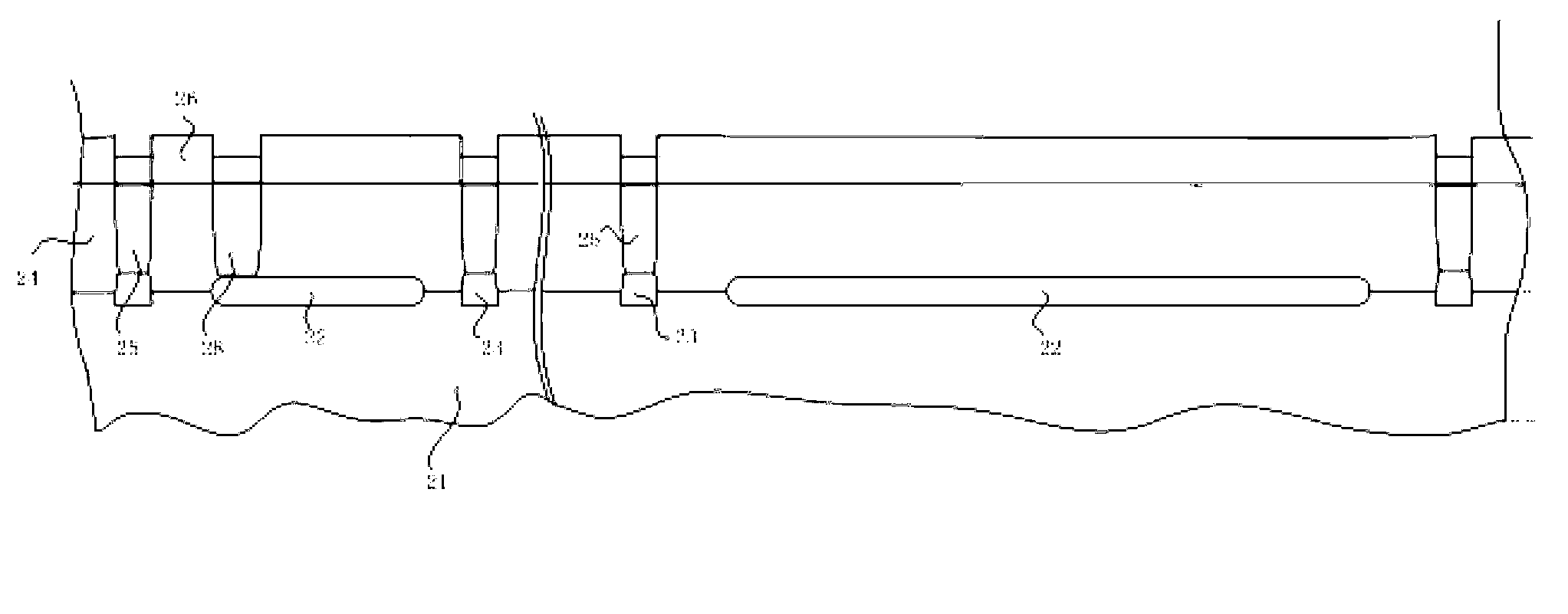
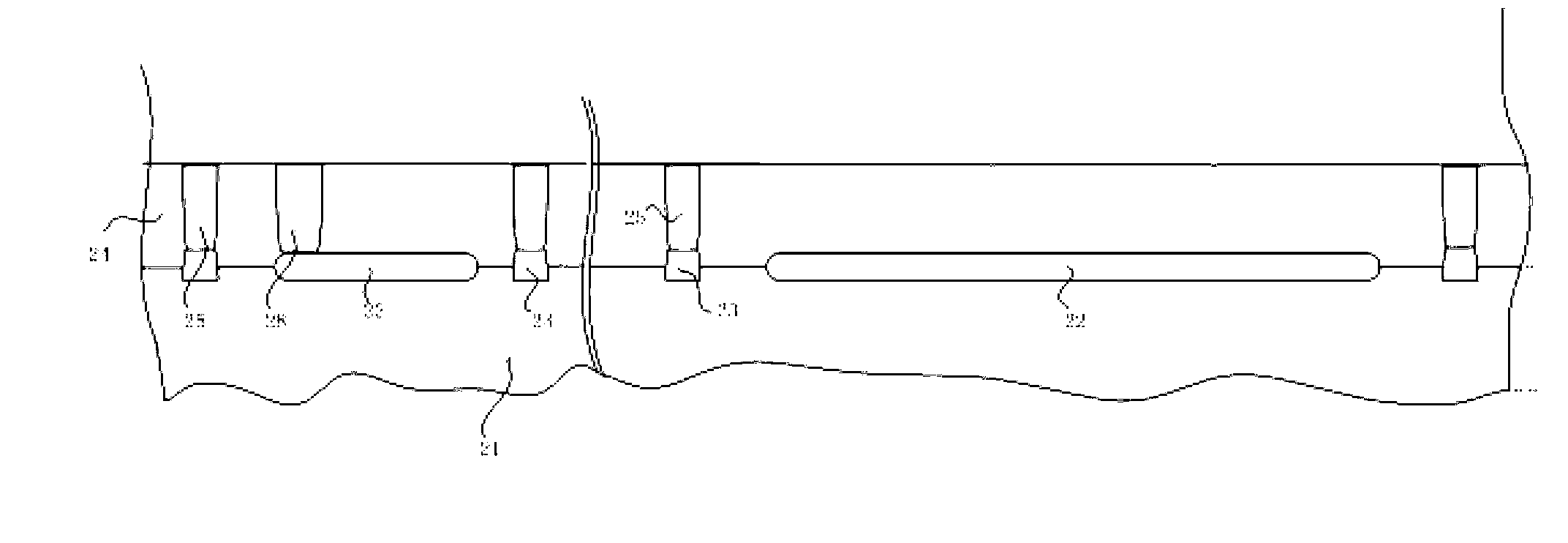
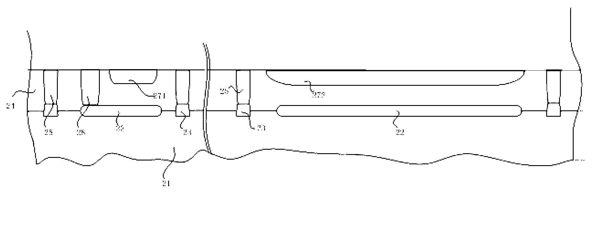
[0043] see Figure 9 , the invention provides a kind of flow process of the manufacturing method of bipolar circuit as:

[0044] S1: Depositing a first dielectric layer on the provided semiconductor substrate, the epitaxial layer of the semiconductor substrate is formed with doped d...


PUM


Abstract

The invention provides a bipolar circuit manufacture method. The bipolar circuit manufacture method includes: depositing a first dielectric layer on a provided semiconductor substrate, and forming doped deep phosphorus, a first-type doped region, a second-type doped region and upper isolation in an epitaxial layer of the semiconductor substrate; combining a contact hole pattern and a capacitive window pattern on a same mask for etching, forming contact holes in the first dielectric layer formed at each level, and forming a required capacitive window in the first dielectric layer on the second-type doped region; and growing a silicon dioxide layer, removing the silicon dioxide layer in part of the selected capacitive window and removing part of the deposited silicon nitride layer to keep the silicon nitride layer in the required capacitive window so as to form different capacitance. The bipolar circuit manufacture method is capable of shortening production time of an annealing process in an emitter region, meets the requirements of high and low voltage modules in a special circuit on capacitance value and capacitive withstood voltage and weakens influences of the emitter region and contact hole photoetching alignment precision on products.

Description

technical field [0001] The invention belongs to the technical field of semiconductor manufacturing technology, and in particular relates to a manufacturing method of a bipolar circuit. Background technique [0002] Traditional bipolar circuit technology employs manufacturing methods combined with flow Figure 1 to Figure 8 To give a detailed explanation: [0003] see figure 1 , forming the bottom layer: select a suitable substrate material 21; form the N-type doped buried layer 22 and the P-type doped lower isolation required for the circuit on the substrate material through oxidation, photolithography, etching, implantation and other processes 23; generate epitaxial layer 24 by epitaxial process; oxidation generation The first oxide layer 26 is used to block the regions that do not need to be doped; a deep phosphorus window is formed in the epitaxial layer 24 by photolithography and etching processes, and is formed by phosphorus diffusion doping, annealing and oxidation...

Claims


Application Information

Patent Timeline
IPC IPC(8): H01L21/768
Inventor 张佼佼李小锋杨彦涛肖金平王铎
Owner HANGZHOU SILAN INTEGRATED CIRCUIT
Why Eureka
Try Eureka