Double-stepped terahertz wave polarization beam splitter
A polarizing beam splitter and stepped technology, applied in the field of terahertz beam splitters, can solve the problems of difficult actual production process, complex structure, low beam splitting rate, etc., and achieve compact structure, high beam splitting rate and small size. Effect
- Summary
- Abstract
- Description
- Claims
- Application Information
AI Technical Summary
Problems solved by technology
Method used
Image
Examples
Embodiment 1
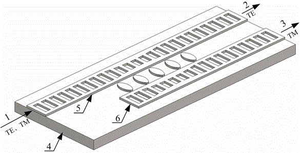
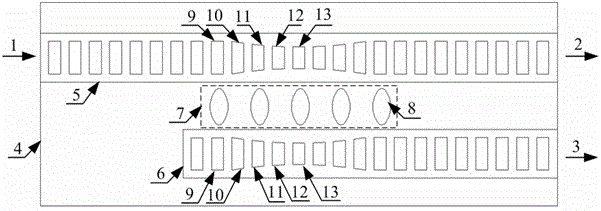
[0016] Double-step terahertz wave polarizing beam splitter:
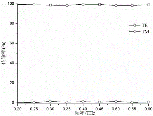
[0017] The material of the substrate is silicon dioxide, the length is 1270 μm, the width is 1000 μm, and the thickness is 400 μm. The materials of the first stepped waveguide, the second stepped waveguide and the elliptical waveguide are all silicon, and the thickness is 80 μm. The lengths of the first stepped waveguide and the second stepped waveguide are 1270 μm and 920 μm respectively, and the widths are both 300 μm. The distance between two adjacent elliptical waveguides of the elliptical waveguide array is 60 μm; the major axis length of the elliptical waveguide is 160 μm, and the minor axis length is 50 μm. The length of the large rectangular groove is 200 μm and the width is 30 μm; the length of the upper base of the first isosceles trapezoidal groove is 170 μm, the length of the lower base is 190 μm, and the height is 30 μm; the length of the upper base of the second isosceles trapezoidal groove is 140 μm ...
PUM
 Abstract
Description
Claims
Application Information
 - R&D
- Intellectual Property
- Life Sciences
- Materials
- Tech Scout
- Unparalleled Data Quality
- Higher Quality Content
- 60% Fewer Hallucinations
Browse by: Latest US Patents, China's latest patents, Technical Efficacy Thesaurus, Application Domain, Technology Topic, Popular Technical Reports.
© 2025 PatSnap. All rights reserved.Legal|Privacy policy|Modern Slavery Act Transparency Statement|Sitemap|About US| Contact US: help@patsnap.com


