New process for controlling array type high-voltage LED side-wall inclination angle

A tilt angle, array-type technology, applied in the direction of electrical components, circuits, semiconductor devices, etc., can solve the problems of increasing HV-LED manufacturing cost, difficult to remove, reducing the yield of HV-LED chips, etc., to achieve cost reduction and easy operation The effect of making and increasing productivity

Inactive Publication Date: 2013-03-27
张庆
View PDF0 Cites 11 Cited by
  • Summary
  • Abstract
  • Description
  • Claims
  • Application Information

AI Technical Summary

Problems solved by technology

However, the reflow process is highly dependent on environmental conditions (sample temperature, ambient humidity, etching process parameters, exposure conditions, etc.), which greatly increases the manufacturing cost of HV-LEDs. In additi

Method used


Image

  • New process for controlling array type high-voltage LED side-wall inclination angle
  • New process for controlling array type high-voltage LED side-wall inclination angle
  • New process for controlling array type high-voltage LED side-wall inclination angle

Examples


Embodiment Construction

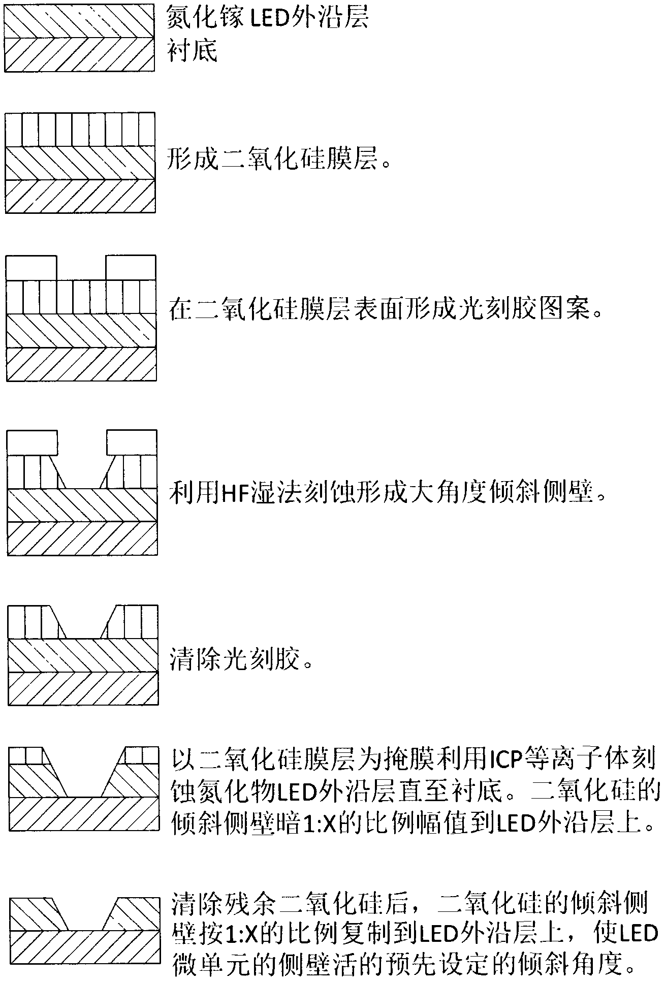
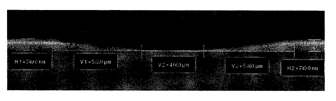
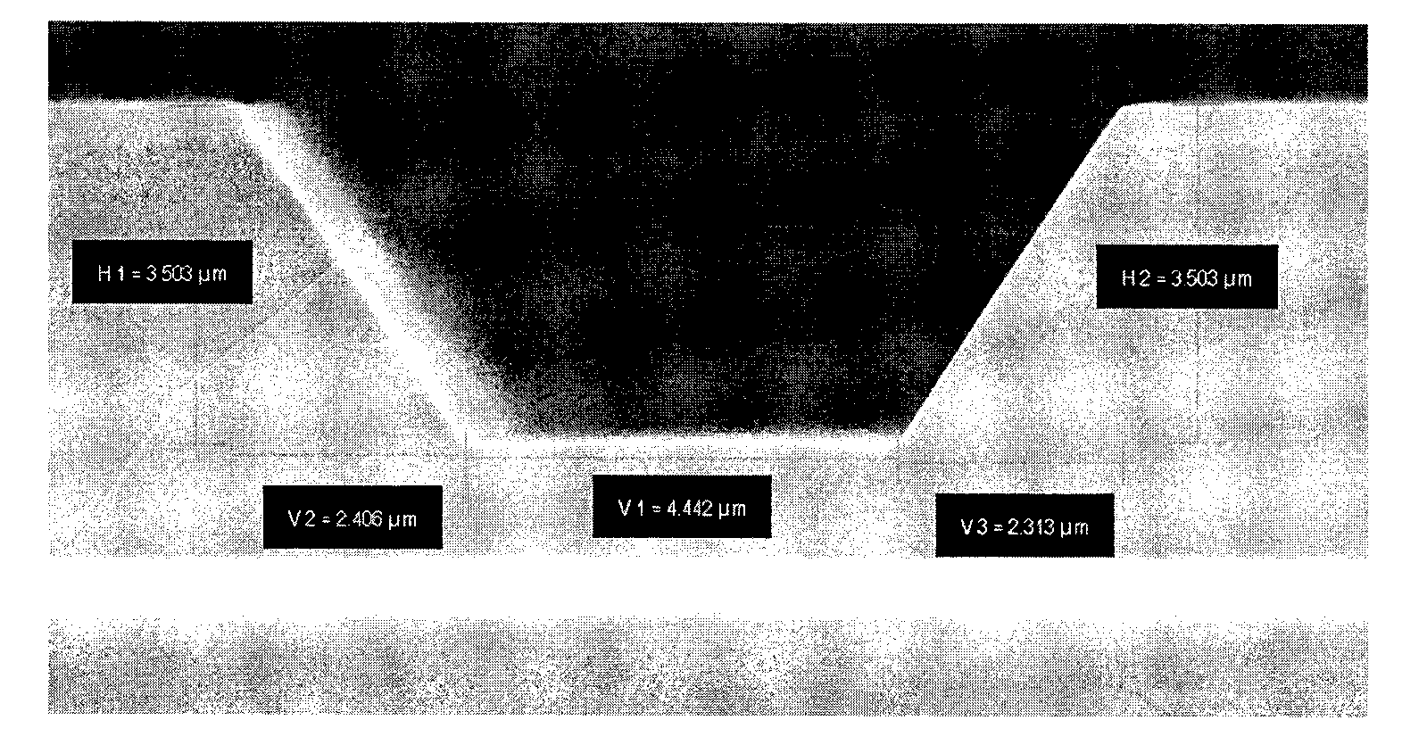
[0019] Implementation example: In this example, through the above-mentioned patented technology, the method of over-wet etching will form a large-angle inclination on the side wall of the silicon dioxide mask, and then copy it to the LED epitaxial layer to realize the micro The inclined sidewall structure of the cell, as an example, the steps are as follows: first, a 1.2 micron silicon dioxide film is formed on the surface of the sapphire-based LED epitaxial heterostructure (epitaxially grown LED heterostructure) by plasma enhanced chemical vapor deposition (PECVD); then , cover the surface of the silicon dioxide film with a photoresist layer (Shipley PR1827) ~ 2.5 microns, and then use a standard photolithography process to form a photoresist pattern; then, using the photoresist pattern as a mask, use a certain proportion of diluted Hydrofluoric Acid (HF) (HF: H2O = 1: 5) etches the silicon dioxide film to form a pre-designed pattern and generate a pre-set angle of inclination...


PUM


Abstract

The invention relates to a new process for controlling side wall inclination angle during manufacturing of array type high-voltage LED chips. The new process includes forming large-angle inclination on a side wall of a silicon dioxide mask by means of wet etching, then copying the large-angle inclination to an LED epitaxial layer, and accordingly forming an inclination side wall structure of micro-units of high-voltage LED chips.

Description

technical field [0001] This patent relates to a new process for controlling the inclination angle of the side wall in the process of manufacturing an array type high-voltage LED chip (HV-LED). Background technique [0002] The recently developed array high-voltage LED chip (HV-LED) technology adopts a new micro-unit array structure. Each micro-unit of the LED chip is surrounded by grooves formed by ion beam etching to emit light independently. , each other through the metal bridge connection to obtain current cascading, through the series-parallel combination to form a pre-designed circuit structure, carrying a predetermined AC and DC (high) voltage, and work to emit light. Therefore, although the single-grain LED light-emitting chip The driving voltage is within 4V, and the HV-LED array design scheme can meet higher driving voltage requirements by changing the number of micro-units and the structure of the series-parallel circuit. Its function and cost performance greatly ...

Claims


Application Information

Patent Timeline
IPC IPC(8): H01L33/00
Inventor 张庆
Owner 张庆
Why Eureka
Try Eureka