Resistor and production method thereof
A manufacturing method and resistance technology, applied in circuits, electrical components, electrical solid devices, etc., can solve problems such as poor operating performance, low resistance and lossless layer effect, improve stability and electrical performance, increase material The effect of selecting and improving process tolerance
- Summary
- Abstract
- Description
- Claims
- Application Information
AI Technical Summary
Problems solved by technology
Method used
Image
Examples
Embodiment Construction
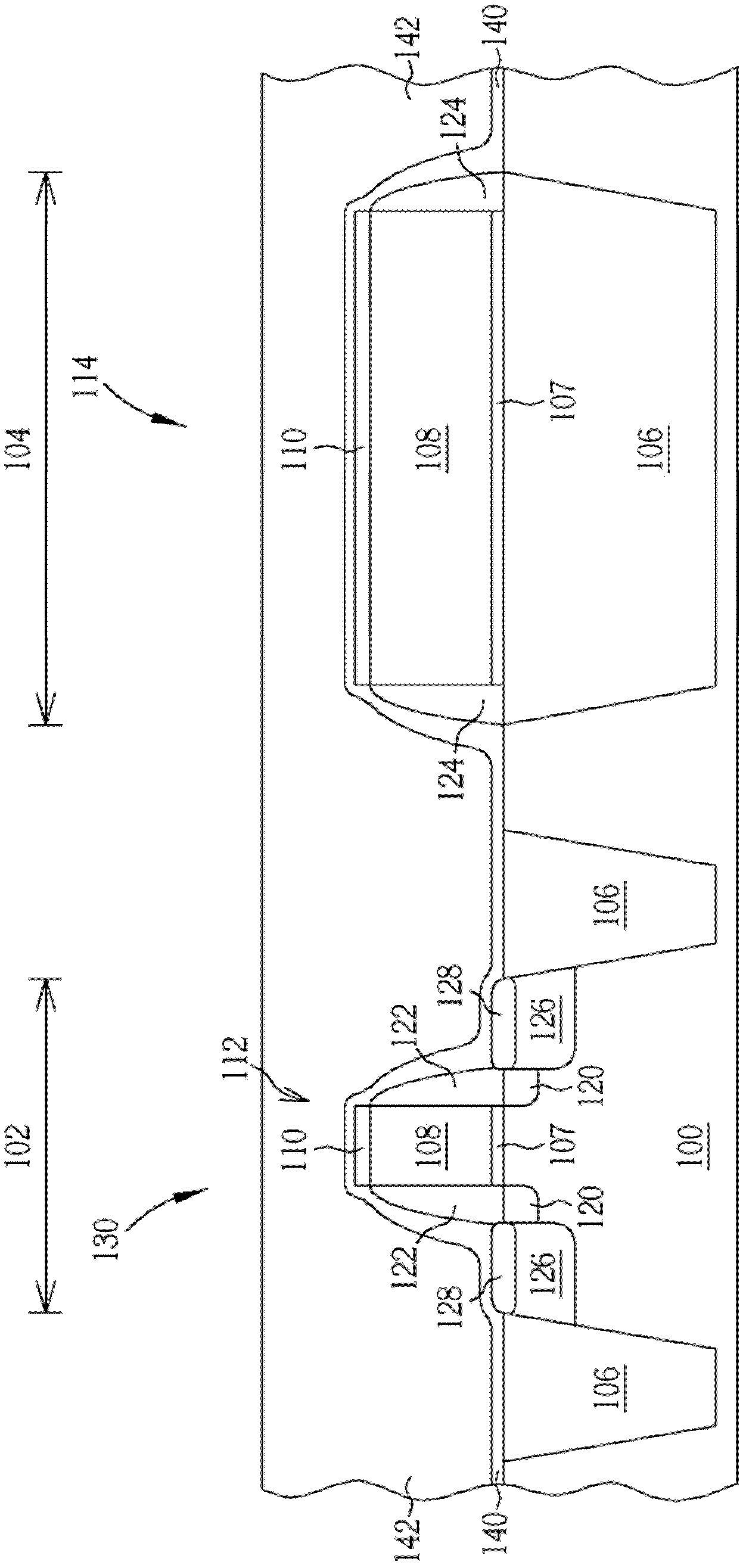
[0025] see Figure 1 to Figure 8 , Figure 1 to Figure 8 It is a schematic diagram of a preferred embodiment of a method for manufacturing a transistor with a metal gate and a resistor provided by the present invention. Such as figure 1 As shown, this preferred embodiment firstly provides a substrate 100, on which a transistor region 102 and a resistor region 104 are defined; a plurality of shallow trench isolations (shallow trench isolation, STI) for providing electrical isolation are formed in the substrate 100 106. And if figure 1 As shown, the resistive area 104 includes an STI 106 used as a location for resistive elements. Next, a dielectric layer 107 , a polysilicon layer 108 , and a patterned hard mask 110 are sequentially formed on the substrate 100 , and the patterned hard mask 110 is used to define gate positions of transistor elements and formation positions of resistor elements. Wherein, the dielectric layer 107 formed between the substrate 100 and the polysil...
PUM
 Abstract
Description
Claims
Application Information
 - R&D
- Intellectual Property
- Life Sciences
- Materials
- Tech Scout
- Unparalleled Data Quality
- Higher Quality Content
- 60% Fewer Hallucinations
Browse by: Latest US Patents, China's latest patents, Technical Efficacy Thesaurus, Application Domain, Technology Topic, Popular Technical Reports.
© 2025 PatSnap. All rights reserved.Legal|Privacy policy|Modern Slavery Act Transparency Statement|Sitemap|About US| Contact US: help@patsnap.com


