Method for fast estimation of lithographic binding patterns in an integrated circuit layout

A technology for determining integrated circuits and layouts, applied in the field of lithography binding patterns for rapid estimation of integrated circuit layouts, and can solve problems such as inapplicability

Active Publication Date: 2013-03-20
INT BUSINESS MASCH CORP
View PDF7 Cites 2 Cited by
  • Summary
  • Abstract
  • Description
  • Claims
  • Application Information

AI Technical Summary

Problems solved by technology

However, such a rule does not apply in general

Method used


Image

  • Method for fast estimation of lithographic binding patterns in an integrated circuit layout
  • Method for fast estimation of lithographic binding patterns in an integrated circuit layout
  • Method for fast estimation of lithographic binding patterns in an integrated circuit layout

Examples


Embodiment Construction

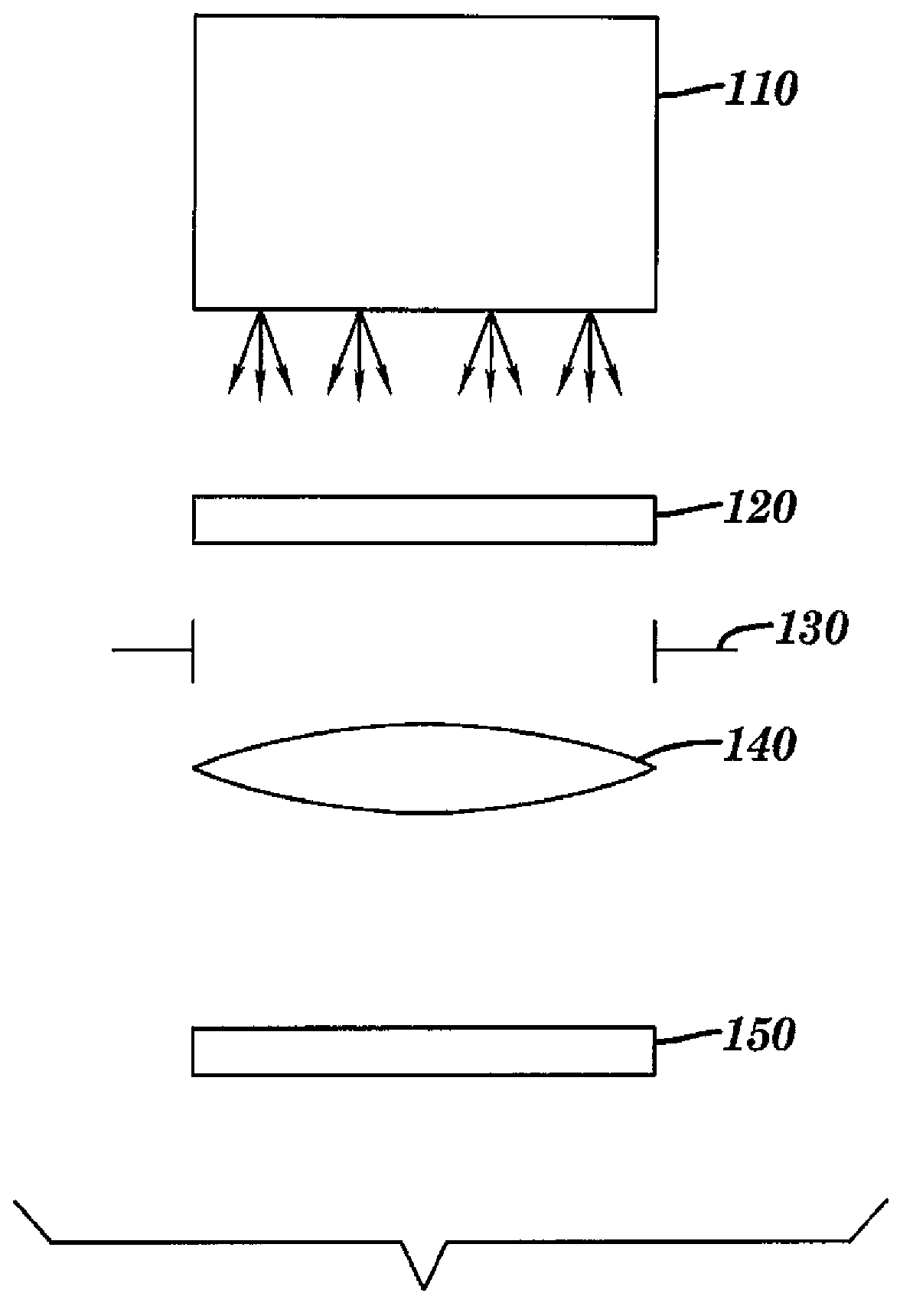
[0037] The present invention provides a method and apparatus for designing and optimizing a layout for use in the manufacture of integrated circuits, and more particularly for identifying and prioritizing portions of the layout for which a full optimization method is to be performed.

[0038] The basic components of a projection lithography system are illustrated in FIG. 1 . An illumination source 110 provides radiation that illuminates a mask 120, also called a reticle; the terms mask and reticle may be used interchangeably. Reticle 120 includes features that act to diffract illuminating radiation through lens 140 that projects an image onto an image plane, eg, semiconductor wafer 150 . The amount of radiation transmitted from reticle 120 to lens 140 may be controlled by pupil 130 . The illumination source 110 may be capable of controlling various source parameters such as direction and intensity. Wafer 150 typically includes a photosensitive material (referred to as resist...


PUM


Abstract

The present invention provides a lithographic difficulty metric that is a function of an energy ratio factor that includes a ratio of hard-to-print energy to easy-to-print energy of the diffraction orders along an angular coordinate [theta]i of spatial frequency space, an energy entropy factor comprising energy entropy of said diffraction orders along said angular coordinate [theta]i, a phase entropy factor comprising phase entropy of said diffraction orders along said angular coordinate 6,, and a total energy entropy factor comprising total energy entropy of said diffraction orders (430, 440).; The hard-to-print energy includes energy of the diffraction orders at values of the normalized radial coordinates r of spatial frequency space in a neighborhood of r=0 and in a neighborhood of r=l, and the easy-to-print energy includes energy of the diffraction orders located at intermediate values of normalized radial coordinates r between the neighborhood of r=0 and the neighborhood of r=l. The value of the lithographic difficulty metric may be used to identify patterns in a design layout that are binding patterns in an optimization computation. The lithographic difficulty metric may be used to design integrated circuits that have good, relatively easy-to-print characteristics.

Description

technical field [0001] The present invention relates broadly to lithographic printing of features for patterning integrated circuits (ICs) on semiconductor chips, and in particular to improvements in the selection and use of illumination source characteristics in combination with diffractive shapes on reticle masks , and more particularly relates to improvements in identifying and prioritizing IC design portions where optimization of lithography processes is performed more economically. Background technique [0002] Photolithographic processes are commonly used in the manufacture of integrated circuits in which radiation is projected through a patterned mask to pattern a wafer to form an image on a light-sensitive material called photoresist or simply resist pattern. The exposed resist material is developed to form openings corresponding to the image pattern, and the pattern is then transferred to the wafer substrate by methods as known in the art, such as etching. [0003...

Claims


Application Information

Patent Timeline
Patent Type & Authority Applications(China)
IPC IPC(8): H01L21/027H01L21/66
CPCG03F1/70G06F30/398G03F7/70483G06F30/20G06F30/30H01L21/0274H01L22/12
Inventor S·巴赫里D·L·德玛里斯M·加布拉尼D·O·梅尔维尔A·E·罗森布鲁斯田克汉
Owner INT BUSINESS MASCH CORP
Why Eureka
Try Eureka