Component substrate and manufacture method thereof

A technology for component substrates and manufacturing methods, applied in semiconductor/solid-state device manufacturing, electrical components, final product manufacturing, etc., can solve problems such as bending and deformation of flexible substrates, achieve stress relief, good water and oxygen resistance, and increase bending Effects of Features

Active Publication Date: 2015-06-17
AU OPTRONICS CORP
View PDF3 Cites 2 Cited by
  • Summary
  • Abstract
  • Description
  • Claims
  • Application Information

AI Technical Summary

Problems solved by technology

Whether it is compressive stress or tensile stress, when the flexible substrate is removed from the glass slide, it may cause the flexible substrate to bend and deform, which increases the risk of subsequent component disconnection or yellow light process misalignment.

Method used


Image

  • Component substrate and manufacture method thereof
  • Component substrate and manufacture method thereof
  • Component substrate and manufacture method thereof

Examples


Embodiment Construction

[0049] The present invention will be described in detail below in conjunction with the accompanying drawings and specific embodiments, but not as a limitation of the present invention.

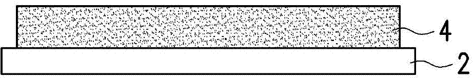
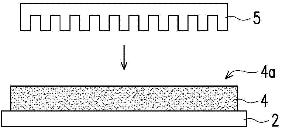
[0050] Figure 1A to Figure 1E It is a schematic diagram of the manufacturing process of the element substrate according to an embodiment of the present invention. Please refer to Figure 1A Firstly, a substrate 4 is formed on a glass substrate 2, wherein the glass substrate 2 may also be other suitable rigid substrates. In this embodiment, the substrate 4 is, for example, a plastic substrate. The substrate 4 is coated by, for example, slot die coating, spin coating, spray coating, and thermal evaporation. In addition, in other embodiments, the substrate 4 may also be a polymer substrate or other suitable flexible substrates.

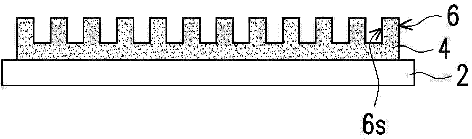
[0051] Next, please refer to Figure 1B as well as Figure 1C , performing a patterning process on the substrate 4 to form a patterned structure 6 on the substrate...


PUM


Abstract

A fabricating method of a device substrate including the following procedures is provided. First, a substrate is provided and a patterned structure is formed on the substrate, wherein the patterned structure includes a plurality of openings. Then, a protective layer is formed on the patterned structure, wherein the protective layer does not fully fill the openings of the patterned structure such that a gap is existed between the protective layer and the patterned structure. Later, a device layer is formed on the protective layer.

Description

technical field [0001] The present invention relates to a substrate and its manufacturing method, and in particular to an element substrate and its manufacturing method. Background technique [0002] In order to possess the characteristic of flexibility, flexible substrates such as plastic substrates or polymer substrates are often used instead of glass substrates for flexible display elements. Due to the poor chemical resistance of the flexible substrate, it is easy to be damaged during the etching process. Therefore, an additional dielectric protection layer (protection layer) is usually required to avoid device damage. The dielectric protection layer can be silicon oxide, aluminum oxide or Inorganic material dielectric layer such as silicon nitride. [0003] In addition to the function of protecting the flexible substrate, these dielectric layers of inorganic materials also have the function of blocking moisture and oxygen. For example, when the subsequent application c...

Claims


Application Information

Patent Timeline
Patent Type & Authority Patents(China)
IPC IPC(8): H01L21/48H01L23/13
CPCH01L21/0217H01L21/02274H01L2224/32145H01L2924/0002H01L2924/12044Y02E10/549Y02P70/50H10K77/111H10K2102/311H01L2924/00H01L23/562H01L21/02107H01L21/48
Inventor 王铮亮洪仕馨胡克龙
Owner AU OPTRONICS CORP
Why Eureka
Try Eureka