
Charge pump circuit and storage

A charge pump and circuit technology, applied in the direction of conversion equipment without intermediate conversion to AC, can solve problems such as multi-power and loss, and achieve the effect of longer working cycle, fewer numbers, and reduced power loss

Inactive Publication Date: 2013-02-20
SHANGHAI HUAHONG GRACE SEMICON MFG CORP
View PDF6 Cites 4 Cited by
  • Summary
  • Abstract
  • Description
  • Claims
  • Application Information

AI Technical Summary

Problems solved by technology

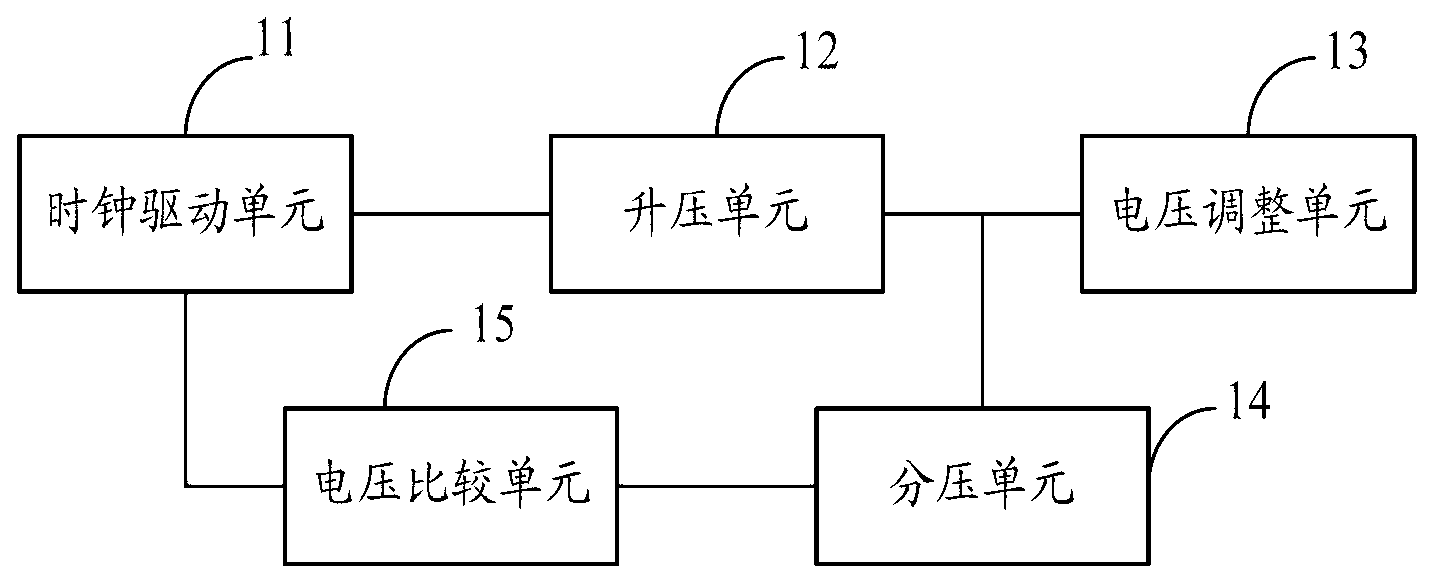
During this process, many devices in the clock drive unit 11 need to be turned on again, thus causing more power loss

Method used


Image

  • Charge pump circuit and storage
  • Charge pump circuit and storage
  • Charge pump circuit and storage

Examples


Embodiment 1

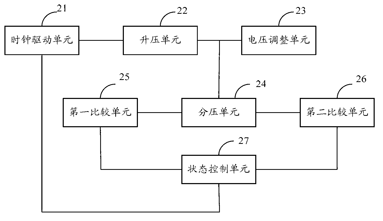
[0037] Figure 4It is a structural diagram of the charge pump circuit of Embodiment 1 of the present invention. refer to Figure 4 , the voltage adjustment unit 23 includes an adjustment transistor MP0, the source of the adjustment transistor MP0 inputs the boosted voltage HV output by the boost unit 22, the gate and the source are connected through a voltage dividing resistor R, and the drain outputs a stable voltage V EP . One terminal of the reference current source I and the filter capacitor C is connected to the gate of the adjustment transistor MP0, and the other terminal is connected to the ground.

[0038] The voltage dividing unit 24 includes a plurality of PMOS transistors connected in series with source and drain electrodes in sequence. The gate and drain of each PMOS transistor are short-circuited, and the substrate is connected to the source. The number of PMOS transistors connected in series is based on the target voltage V of the boost voltage HV set and th...

Embodiment 2

[0051] Figure 6 Shown is the structural diagram of the charge pump circuit of Embodiment 2 of the present invention. refer to figure 2 , the circuit structure of embodiment 2 of the charge pump circuit of the present invention is substantially the same as that of embodiment 1, the difference is that the first divided voltage V D1 and the second divided voltage V D2 are two different voltages provided by the voltage dividing unit 24 . refer to Figure 6 circuit, after the lower limit value V1 and upper limit value V2 of the boost voltage HV are determined, the first reference voltage V can be determined REF1 and the second reference voltage V REF2 The values ​​of are respectively 0.8V and 1.7V.

[0052] The working principle of the charge pump circuit in Embodiment 2 is completely the same as that in Embodiment 1, and will not be repeated here.

[0053] The embodiment of the present invention also provides a memory, including the charge pump circuit provided in the abo...


PUM


Abstract

Provided are a charge pump circuit and a storage. The charge pump circuit comprises a clock driving unit, a boosting unit, a voltage adjustment unit, a voltage dividing unit, a first comparison unit, a second comparison unit and a state control unit. The voltage dividing unit outputs first divided voltage and second divided voltage. The first comparison unit is used for comparing the first divided voltage and first reference voltage and outputting a first comparison result. The second comparison unit is used for comparing the second divided voltage and second reference voltage and outputting a second comparison result. The state control unit is used for outputting control level to the clock driving unit according to the first comparison result and the second comparison result and controlling the clock driving unit to output driving voltage. According to the technical scheme, power loss of the clock driving unit is reduced by reducing awaking times of the clock driving unit.

Description

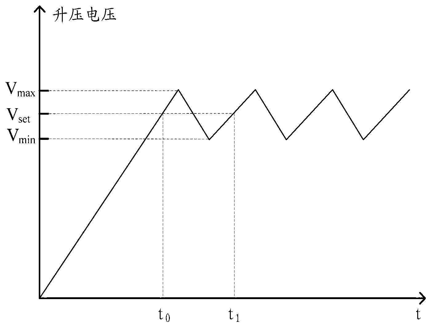
technical field [0001] The invention relates to the technical field of semiconductors, in particular to a charge pump circuit and a memory. Background technique [0002] With the development of semiconductor technology, based on the design requirements of low power consumption and low cost, the power supply voltage of the memory is usually relatively low, such as 2.5V, 1.8V and so on. However, in order to realize reading and writing of stored information, a programming voltage and an erasing voltage much higher than the power supply voltage are usually required, such as 8V, 11V, and the like. Therefore, charge pump circuits are widely used in memories to obtain higher programming voltages and erasing voltages with lower power supply voltages. [0003] refer to figure 1 , shows a structural diagram of an existing charge pump circuit. Such as figure 1 As shown, the existing charge pump circuit includes: a clock driving unit 11 , a voltage boosting unit 12 , a voltage adjus...

Claims


Application Information

Patent Timeline
Patent Type & Authority Applications(China)
IPC IPC(8): H02M3/07
Inventor 杨光军胡剑
Owner SHANGHAI HUAHONG GRACE SEMICON MFG CORP
Learn More