Trenched Schottky-barrier diode and manufacturing method thereof
A Schottky potential and diode technology, used in semiconductor/solid-state device manufacturing, electrical components, circuits, etc., can solve the problems of large reverse leakage, poor reverse blocking ability, low performance and reliability, and achieve low The effect of reduced requirements on reverse leakage, high voltage reverse blocking capability, absolute thickness and relative thickness uniformity
- Summary
- Abstract
- Description
- Claims
- Application Information
AI Technical Summary
Problems solved by technology
Method used
Image
Examples
Embodiment 1
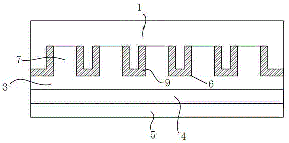
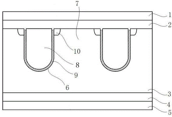
[0046] Such as figure 2 As shown, a trench Schottky barrier diode consists of an anode metal layer 1, a lightly doped epitaxial layer 3 of the first conductivity type, a substrate 4, and a cathode that form an ohmic contact with each other from top to bottom. The metal layer 5 is composed of the substrate 4 and the epitaxial layer 3, both of which are monocrystalline silicon. The upper part of the epitaxial layer 3 is horizontally carved with a number of grooves 6, and the epitaxial layer 3 between adjacent grooves 6 forms a boss 7. The epitaxial layer 3 The impurity doping concentration increases from the top surface to the bottom surface, where the top surface doping concentration is 10 16 cm -3 , the bottom doping concentration is 10 21 cm -3 A Schottky barrier metal layer 2 with a thickness of 10 angstroms is evaporated between the anode metal layer 1 and the epitaxial layer 4, and the Schottky barrier metal layer 2 forms a Schottky barrier contact with the top surfa...
Embodiment 2
[0061] The trench Schottky barrier diode structure of this embodiment is the same as that of Embodiment 1, except that the thickness of the Schottky barrier metal layer 2 in this embodiment is 500 angstroms, and the doping concentration of the top surface of the epitaxial layer 3 is for 10 15 cm -3 , the bottom doping concentration is 10 20 cm -3 , the top surface doping concentration of conductive polysilicon 8 is 10 19 cm -3 , the bottom doping concentration is 10 15 cm -3 .
[0062] The rest of the steps in the method for manufacturing trench Schottky barrier diodes in this embodiment are the same as those in Embodiment 1, except that the etching rate ratio between the isolation layer 9 and the hard mask 11 is controlled during wet etching in step (10). 1:50.
Embodiment 3
[0064] The structure of the trench Schottky barrier diode in this embodiment is the same as that in Embodiment 1.
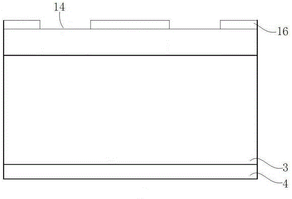
[0065]The remaining steps in the manufacturing method of trench Schottky barrier diodes in this embodiment are the same as those in Embodiment 1, except that the doping method of the conductive polysilicon 8 and the corner protection region 10 in step (9) is different. Step (nine) of the embodiment is: as Figure 9 As shown, the doped glass layer 13 is firstly deposited on the exposed corner top surface of the boss 7 and the top surface of the polysilicon 15 by high-temperature diffusion method, and after thermal annealing, the doped glass layer 13 is selectively removed by wet etching to form Conductive polysilicon 8, and at the same time form corner protection regions 10.
PUM
| Property | Measurement | Unit |
|---|---|---|
| thickness | aaaaa | aaaaa |
| thickness | aaaaa | aaaaa |
| thickness | aaaaa | aaaaa |
Abstract
Description
Claims
Application Information
 - R&D
- Intellectual Property
- Life Sciences
- Materials
- Tech Scout
- Unparalleled Data Quality
- Higher Quality Content
- 60% Fewer Hallucinations
Browse by: Latest US Patents, China's latest patents, Technical Efficacy Thesaurus, Application Domain, Technology Topic, Popular Technical Reports.
© 2025 PatSnap. All rights reserved.Legal|Privacy policy|Modern Slavery Act Transparency Statement|Sitemap|About US| Contact US: help@patsnap.com


