Titanium dioxide photo-catalyzed film and preparation method thereof
A photocatalytic thin film, titanium dioxide technology, applied in ion implantation plating, electrolytic coating, surface reaction electrolytic coating, etc., can solve the problems such as not found, and achieve large specific surface area, excellent photocatalytic performance, excellent light transmittance and light The effect of catalytic performance
- Summary
- Abstract
- Description
- Claims
- Application Information
AI Technical Summary
Problems solved by technology
Method used
Image
Examples
Embodiment 1
[0047] (1) Deposition of titanium film on FTO glass by magnetron sputtering
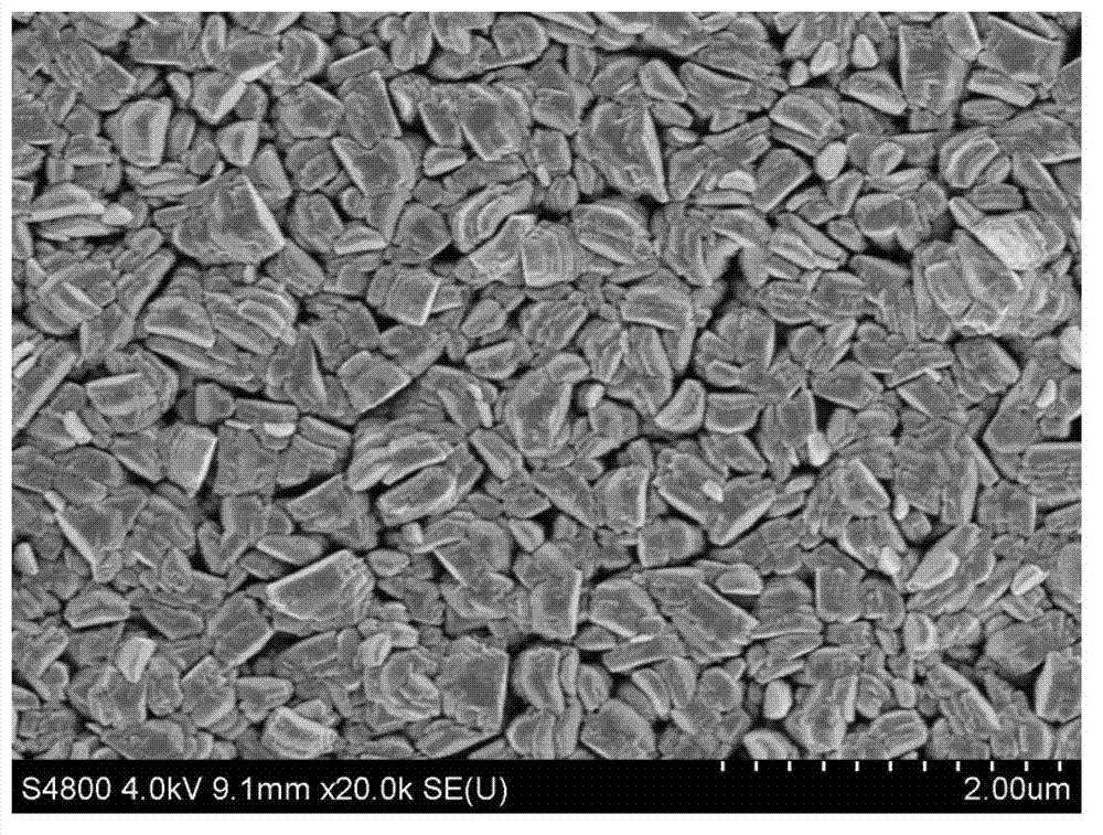
[0048] Sputtering deposition of titanium film: In the deposition chamber, the background pressure of the deposition chamber is 5×10 -5 Pa. A DC power supply is used, the Ti target is installed on the cathode, the glass substrate is installed on the anode, and the distance between the Ti target and the glass substrate is 62mm. Introduce Ar gas, adjust the chamber pressure to 0.1Pa, and the power density of the Ti target to 3.7w / cm 2 . At room temperature (20°C), the titanium film was deposited by sputtering on the substrate for 22 minutes to obtain a titanium film with a columnar structure with a thickness of 510nm and a column width of 100-200nm. The XRD pattern of the titanium film shows that the diffraction intensities of the (002) plane and (101) plane are I(002) and I(101) respectively, these values satisfy I(002)>I(101), and the film layer is in the (002) Preferential growth on the crystal...
Embodiment 2
[0055] (1) Deposit titanium film on ordinary glass by magnetron sputtering method
[0056] Sputtering deposition of titanium film: In the deposition chamber, the background pressure of the deposition chamber is 5×10 -4 Pa. AC power is used, the Ti target is installed on the cathode, the glass substrate is installed on the anode, and the distance between the Ti target and the glass substrate is 75mm. Introduce Ar gas, adjust the chamber pressure to 1Pa, and the power density of the Ti target to 6.2w / cm 2 . At 30°C, the titanium film was deposited by sputtering on the substrate, and the deposition time was 16 minutes to obtain a columnar titanium film with a thickness of 420nm and a column width of 400-500nm. The XRD pattern of the titanium film shows that the diffraction intensities of the (002) plane and (101) plane are I(002) and I(101) respectively, these values satisfy I(002)>I(101), and the film layer is in the (002) Preferential growth on the crystal face. The SEM ...
Embodiment 3
[0063] (1) Deposit titanium film on ordinary glass by magnetron sputtering method
[0064] Sputtering deposition of titanium film: In the deposition chamber, the background pressure of the deposition chamber is 1×10 -4 Pa. A DC power supply is used, the Ti target is installed on the cathode, the glass substrate is installed on the anode, and the distance between the Ti target and the glass substrate is 62mm. Introduce Ar gas, adjust the chamber pressure to 0.5Pa, and the power density of the Ti target to 4.3w / cm 2 . At 30° C., a titanium film was sputter-deposited on the substrate for 18 minutes to obtain a columnar titanium film with a thickness of 468 nm and a column width of 300 nm. The XRD pattern of the titanium film shows that the diffraction intensities of the (002) plane and (101) plane are I(002) and I(101) respectively, these values satisfy I(002)>I(101), and the film layer is in the (002) Preferential growth on the crystal face. The SEM image of the titanium ...
PUM
| Property | Measurement | Unit |
|---|---|---|
| length | aaaaa | aaaaa |
| width | aaaaa | aaaaa |
| thickness | aaaaa | aaaaa |
Abstract
Description
Claims
Application Information
 - R&D Engineer
- R&D Manager
- IP Professional
- Industry Leading Data Capabilities
- Powerful AI technology
- Patent DNA Extraction
Browse by: Latest US Patents, China's latest patents, Technical Efficacy Thesaurus, Application Domain, Technology Topic, Popular Technical Reports.
© 2024 PatSnap. All rights reserved.Legal|Privacy policy|Modern Slavery Act Transparency Statement|Sitemap|About US| Contact US: help@patsnap.com


