
Machining method of metal packaging shell of large-scale and large-power integrated circuit

An integrated circuit and metal packaging technology, which is applied in the manufacture of circuits, electrical components, semiconductors/solid-state devices, etc., can solve the problem of not being able to reach industrial production, not fully satisfying the processing of large-scale high-power integrated circuit shells, and not fully satisfying the product environment Adaptability and other issues

Active Publication Date: 2015-04-08
中国电子科技集团公司第四十研究所
View PDF1 Cites 3 Cited by
  • Summary
  • Abstract
  • Description
  • Claims
  • Application Information

AI Technical Summary

Problems solved by technology

[0006] When the processing technology of the above-mentioned small-scale and low-power integrated circuit shells is applied to the processing of large-scale, high-power integrated circuit shells, the following problems will occur: 1. Because the large-scale, high-power integrated circuit shells are large in size, the bottom plate The size is about 80mm long x 70mm wide, and the cavity volume reaches about 70cm 3 , the number of leads is 40-50. If the base plate is made by stamping technology, the base plate produced will be rough and uneven, and the precision cannot meet the requirements, such as the overall size, the steps around the base plate, the through hole for placing the glass blank, and the smoothness. , chamfering of each side, etc. often fail to meet the requirements, resulting in the final airtightness of the product is not easy to meet the requirements, and because the shape and flatness of each bottom plate after stamping and forming cannot be kept consistent, the subsequent process changes. Difficult to obtain, unable to meet the requirements of industrial production
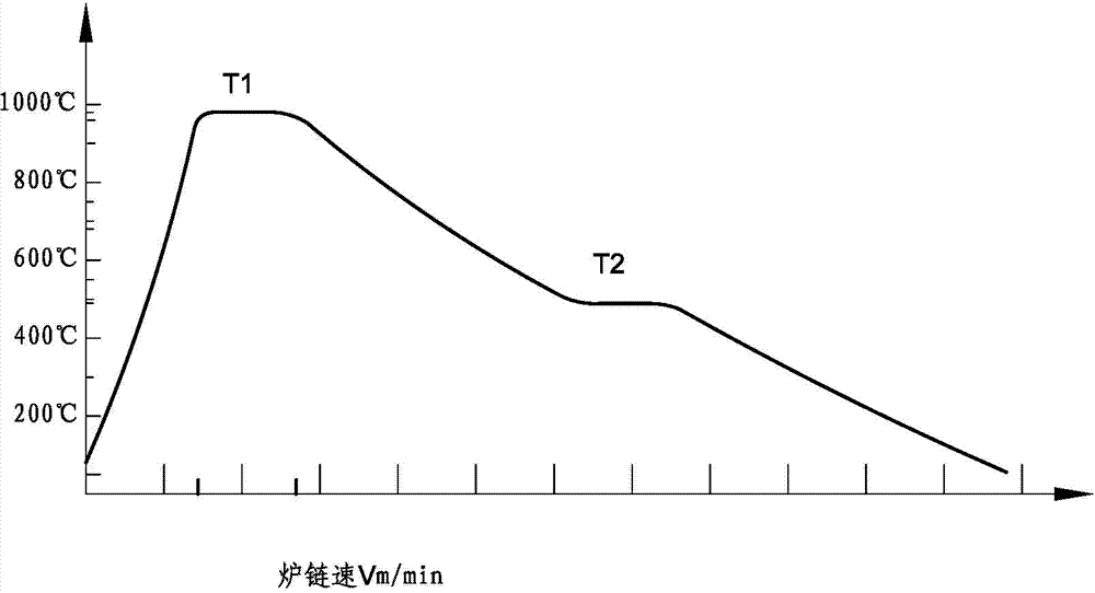
2. The existing sintering and annealing of the base is directly annealed after heating up to 1000°C for a period of time. This process cannot fully meet the processing of the base of the large-scale and high-power integrated circuit shell, and cannot fully meet the environmental adaptability requirements of the product.

Method used


Image

  • Machining method of metal packaging shell of large-scale and large-power integrated circuit
  • Machining method of metal packaging shell of large-scale and large-power integrated circuit
  • Machining method of metal packaging shell of large-scale and large-power integrated circuit

Examples


Embodiment 1

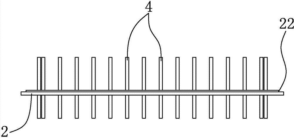
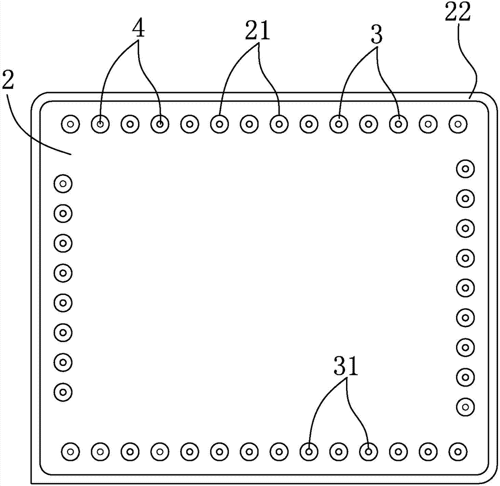
[0046] For the processing method of large-scale and high-power integrated circuit metal packaging shell, see figure 2 — Figure 5 , the shell includes a base and an outer cover 1, the base is composed of a base plate 2, forty-five glass blanks 3, and forty-five lead pins 4, and the base plate 2 is provided with forty-five pins for placing lead pins 4 and glass blanks. 3 through the first through hole 21, the lead pin 4 is placed in the first through hole 21 on the bottom plate 2 through the glass gob 3;

[0047] The processing method of the base includes the following process steps:

[0048] (1) Use the processing center LMC-1000 to process the Kovar alloy sheet material 4J29 into a rectangular bottom plate 2 with forty-five first through holes 21 for placing the lead pins 4 and the glass blank 3. The periphery of the bottom plate 2 is provided with Place the step 22 of the outer cover 1, after the machining is completed, sandblast the surface of the bottom plate 2, and then ...

Embodiment 2

[0057] For the processing method of large-scale and high-power integrated circuit metal packaging shell, see figure 2 — Figure 5 , the shell includes a base and an outer cover 1, the base is composed of a base plate 2, forty-five glass blanks 3, and forty-five lead pins 4, and the base plate 2 is provided with forty-five pins for placing lead pins 4 and glass blanks. 3 through the first through hole 21, the lead pin 4 is placed in the first through hole 21 on the bottom plate 2 through the glass gob 3;

[0058] The processing method of the base includes the following process steps:

[0059] (1) Use the processing center LMC-1000 to process the Kovar alloy sheet material 4J29 into a rectangular bottom plate 2 with forty-five first through holes 21 for placing the lead pins 4 and the glass blank 3. The periphery of the bottom plate 2 is provided with Place the step 22 of the outer cover 1, after the machining is completed, sandblast the surface of the bottom plate 2, and the...


PUM


Abstract

The invention relates to a machining method of a metal packaging shell of a large-scale and large-power integrated circuit. The shell comprises a base and an outer cover, wherein the base is composed of a base plate, a plurality of glass blanks and a plurality of terminal pins; a plurality of first through holes for holding the terminal pins and the glass blanks are formed on the base plate; and the terminal pins are arranged inside the first through holes on the base plate through the glass blanks. When the base and the outer cover are machined well, required elements such as integrated circuits and modules are installed on the base; and the outer cover is welded with the base; the integrated circuits, the modules and the like are fixed on the base of the metal shell, and are connected with external tested devices through leading-out terminals of the terminal pins, thereby accomplishing the output, input and detection and control functions of system signals. The outer cover is welded with the base; the integrated circuits and the modules are sealed inside the metal shell, so that both the functions of signal output, detection and control are achieved, and the internal circuit is prevented from being influenced by various external severe environments.

Description

technical field [0001] The invention relates to a processing method for a large-scale, high-power integrated circuit metal packaging shell. Background technique [0002] Integrated circuits are widely used in aviation, communications, electronics, shipping and other fields. They are mainly used in the control systems of various weapons and electronic equipment and instruments of the Army, Navy, and Armed Police. They are one of the key components of new equipment. . The casing is a key part of integrated circuits and hybrid integrated circuits, and its quality and performance will directly affect the quality and performance of hybrid integrated circuits. The function of the shell is to connect, integrate, and seal the integrated circuits and modules in the shell, which not only transmits signals but also protects the circuits inside, so that the modules are not affected by the harsh external environment. Due to the large size of the packaging shell of large-scale and high-...

Claims


Application Information

Patent Timeline
Patent Type & Authority Patents(China)
IPC IPC(8): H01L21/48
Inventor 杨俊钊刘燕刘彬蒙高安江洪涛张斌
Owner 中国电子科技集团公司第四十研究所
Learn More