Thin substrate, mass-transfer bernoulli end-effector

一种端拾器、基片的技术,应用在半导体/固态器件制造、夹头、机械手等方向,能够解决增加真空管道系统复杂度、增加保持器成本等问题

Active Publication Date: 2015-05-13
SHANGHAI FORTREND TECH CO LTD
View PDF6 Cites 0 Cited by
  • Summary
  • Abstract
  • Description
  • Claims
  • Application Information

AI Technical Summary

Problems solved by technology

[0005]2. Potential repositioning of the wafers; and
It can be seen that solving this problem with a direct vacuum suction substrate holder increases the complexity of the vacuum piping system proportional to the number of substrates that need to be processed per batch, and correspondingly increases the cost of the holder

Method used


Image

  • Thin substrate, mass-transfer bernoulli end-effector
  • Thin substrate, mass-transfer bernoulli end-effector
  • Thin substrate, mass-transfer bernoulli end-effector

Examples


Embodiment Construction

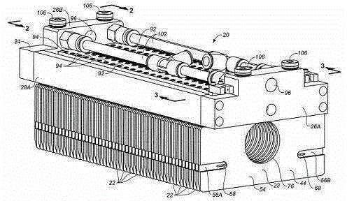
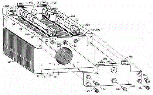
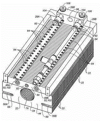
[0066] figure 1 Shown is a specific embodiment of the currently optimal batch transfer end effector represented by serial number 20, which is suitable for transferring a batch of thin semiconductor substrates at the same time. The end effector 20 includes a plurality of juxtaposed suction-finger substrate holders 22 , and a rectangular end-effector frame 24 surrounds and supports the upper half of the group of suction-finger substrate holders 22 . The end effector frame 24 includes a pair of end plates 26A, 26B at opposite ends of the end effector frame 24 and oriented parallel to the substrate holder 22 . Such as figure 2 and image 3 As shown, a pair of side rails 28A, 28B extend between opposite ends of the end panels 26A, 26B. Such as figure 2 As shown, a pair of fasteners 32 secure two ends of the end panels 26A, 26B to corresponding adjacent ends of the side rails 28A, 28B to establish the end effector frame 24 .

[0067] Figure 4 Indicated to include Figure 1...


PUM


Abstract

An end effector (20, 20') for simultaneously transferring a batch of substrates (202). The end effector (20, 20') includes a set of juxtaposed substrate grippers (22, 22') having a pitch between pairs of grippers (22, 22'') that does not exceed six (6.00) mm. Each gripper (22, 22') has a contact surface (54, 54') against which a substrate (202) becomes clamped upon injecting a gaseous jet into an open groove (56A, 56B, 56') formed into the contact surface (54, 54'). Due to the close spacing between immediately adjacent pairs of substrate grippers (22, 22'), the open groove (56A, 56B, 56') must be very shallow. The open groove (56A, 56B, 56') can be characterized by having a groove depth into the contact surface (54, 54') that is between two (2 .00) mm and two and four tenths (2.40) mm. Alternatively, the open groove (56A, 56B, 56') can be characterized by having a groove width at the contact surface (54, 54') that is at least three (3) times larger than a groove depth into the contact surface of the substrate gripper.

Description

technical field [0001] The invention belongs to the technical field of semiconductor processing, in particular to the processing of semiconductor wafers / substrates. Background technique [0002] Some semiconductor wafer processing operations require loading many disk-shaped wafers into a process carrier in a specific orientation. Examples of such processes are "wet process" processing and horizontal diffusion furnace processing. Typically, integrated circuit (IC) fabrication tools process 100 wafers up to a maximum of 500 wafers per hour. Therefore, most integrated circuit fabrication tools utilize a single substrate transfer. In contrast, silicon solar cell manufacturing requires a minimum throughput of 1600 wafers per hour. Many solar cell manufacturing tools actually require transfers of 3,000 wafers per hour. Therefore, solar cell manufacturing requires the transfer of large batches of semiconductor substrates. [0003] Wafers typically prepared for processing requi...

Claims


Application Information

Patent Timeline
Patent Type & Authority Patents(China)
IPC IPC(8): B25J15/00B25J15/06
CPCB25J15/0616H01L21/67742H01L21/67766H01L21/6838
Inventor K.C.吴闻静杨瑞秋郑君强
Owner SHANGHAI FORTREND TECH CO LTD
Why Eureka
Try Eureka