
Exposure device and method of same

An exposure device and exposure method technology, applied in the field of interference exposure and exposure, can solve the problems of inability to effectively adjust the resolution, achieve the effect of continuously adjustable pitch, and improve the utilization rate of energy

Active Publication Date: 2012-10-17
SHANGHAI MICRO ELECTRONICS EQUIP (GRP) CO LTD
View PDF8 Cites 8 Cited by
  • Summary
  • Abstract
  • Description
  • Claims
  • Application Information

AI Technical Summary

Problems solved by technology

[0008] The technical problem to be solved by the present invention is that the prior art cannot effectively adjust the resolution in exposure within a continuous range

Method used


Image

  • Exposure device and method of same
  • Exposure device and method of same
  • Exposure device and method of same

Examples


Embodiment 1

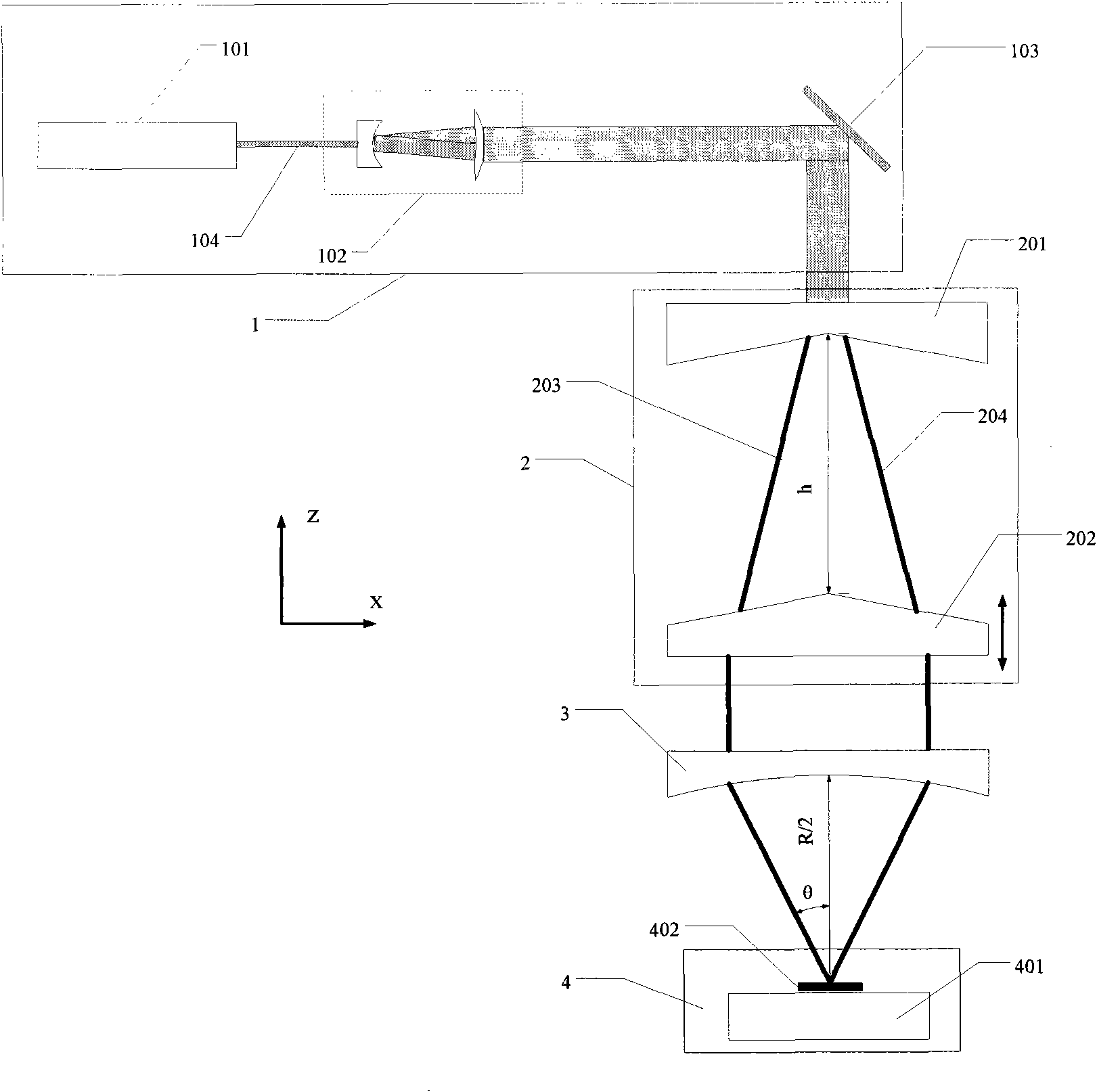
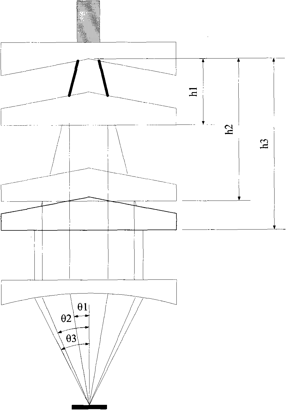
[0029] see figure 1 and 2 As shown, an interference exposure device with continuously adjustable resolution in this embodiment includes four parts: an illumination unit 1, a prism assembly 2, an interference head 3, and a stage unit 4. The z direction in the figure is the opposite direction along the optical path. The x direction is the horizontal right direction, and the x direction to the z direction satisfy the right-hand law.

[0030] Wherein, the illumination unit 1 includes a light source 101, a beam expander 102 and a reflector 103; the prism set 2 is composed of two wedge prisms 201, 202; the interference head 3 is a curved mirror; the stage unit 4 includes a slide table 401 and The carried substrate 402 may specifically be a glue-coated substrate.

[0031] The working process of the device is as follows:

[0032] A light source 101 (usually a laser) emits a parallel coherent beam 104 with a wavelength of λ, which is expanded by a beam expander 102 to form a spot of...

Embodiment 2

[0045] Another embodiment of the interference exposure device of the present invention is as Figure 5 As shown, it includes an illumination unit 1 , a prism set 2 , an interference head 3 ′, a wafer stage 401 and a base.

[0046] The difference between this embodiment and Embodiment 1 lies in the different interference heads used. The interference head 3' in this embodiment is a prism, its incident surface and outgoing surface are planes, and the reflection surfaces on both sides are paraboloids. Record its appearance for:

[0047] x 2 =2p(z-c)p>0 (4)

[0048] Among them, p is the focal length, c is the distance between the vertex of the paraboloid and the x-axis, and the exit surface passes through the focal point of the paraboloid Therefore, according to the properties of the paraboloid, it can be known that all parallel incident light beams converge at the focal plane where the focus of the paraboloid is located, so no matter how the resolution is adjusted, the converg...


PUM


Abstract

An exposure device and a method of the same are disclosed. The device comprises an illuminating unit sending out a coherent beam; a prism set through which the coherent beam is gathered into a plurality of parallel interference arms, and the plurality of parallel interference arms are sent out; an interference head which interferes in the parallel interference arms and makes them form interference fringes; and a base, the interference fringes are located on the surface of the base. The device is characterized in that the prism set comprises a first prism and a second prism, and spacing between the first prism and the second prism along on an optical propagation direction can be adjusted, and the height of the parallel interference arms gathered by the interference head is constant.

Description

technical field [0001] The invention relates to the field of exposure, in particular to the field of interference exposure. Background technique [0002] Under the background that the critical dimension (Critical dimension) in the IC field generally enters below 90nm, using the method of optical projection exposure, in order to produce high-resolution periodic patterns within a certain exposure field range, a high-resolution mask is required , and equipped with a large numerical aperture (NA) objective lens, resulting in a smaller depth of focus; and as the size of the substrate becomes larger, it is often difficult to guarantee the flatness of the substrate, such as 12-inch silicon wafers, sapphire substrates, etc. , so it is necessary to introduce a complex, high-precision focusing and leveling system to ensure that the exposure surface is within the focal depth range of the projection objective lens; in addition, resolution enhancement technology (Resolution Enhancement T...

Claims


Application Information

Patent Timeline
Patent Type & Authority Applications(China)
IPC IPC(8): G03F7/20
Inventor 许琦欣王帆
Owner SHANGHAI MICRO ELECTRONICS EQUIP (GRP) CO LTD
Learn More