Test structure and test method for negative bias temperature instability of semiconductor device

A technology of instability and test structure, applied in the field of test structure of semiconductor device negative bias temperature instability, can solve problems such as the difficulty of applying the instantaneous test method and the inability of the source measurement unit to test the use of the machine, so as to avoid recovery. effect, the effect of improving accuracy

Active Publication Date: 2014-11-26
SEMICON MFG INT (SHANGHAI) CORP
View PDF3 Cites 0 Cited by
  • Summary
  • Abstract
  • Description
  • Claims
  • Application Information

AI Technical Summary

Problems solved by technology

However, the transient test method requires a special source measure unit (SMU, Power Source Measure Unit) when performing a wafer-level reliability (WLR, Wafer Level Reliability) test, and the source measure unit cannot be used on a traditional test machine ; and for package level reliability (PLR, Package Level Reliability) test, due to the limitation of parallel test, this transient test method is difficult to obtain application

Method used


Image

  • Test structure and test method for negative bias temperature instability of semiconductor device
  • Test structure and test method for negative bias temperature instability of semiconductor device
  • Test structure and test method for negative bias temperature instability of semiconductor device

Examples


Embodiment Construction

[0032] The test structure and test method for the negative bias temperature instability of semiconductor devices proposed by the present invention will be further described in detail below with reference to the accompanying drawings and specific embodiments. Advantages and features of the present invention will be apparent from the following description and claims. It should be noted that all the drawings are in very simplified form and use imprecise ratios, which are only used for the purpose of conveniently and clearly assisting in describing the embodiments of the present invention.
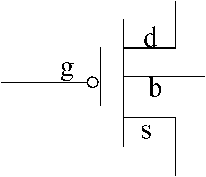
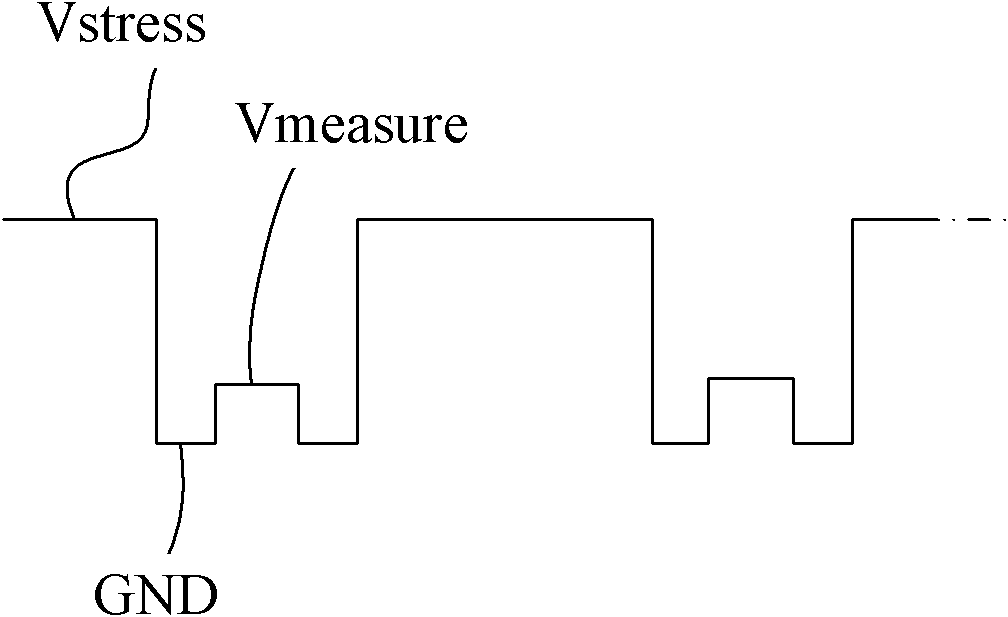
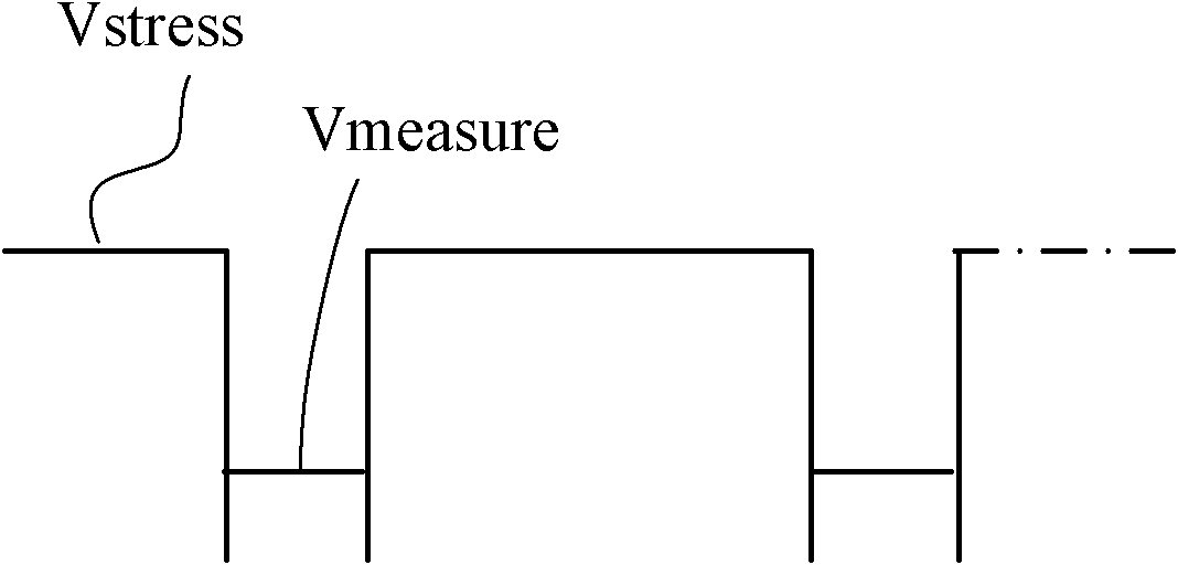
[0033] The core idea of ​​the present invention is to provide a semiconductor device negative bias temperature instability test structure, the structure includes a bias output device, the voltage of the bias output device on the grid is negatively biased by the stress During the transition from the voltage to the test voltage or from the test voltage to the stress negative bias, a sustain volt...


PUM


Abstract

The invention discloses a test structure for negative bias temperature instability (NBTI) of a semiconductor device. The test structure includes a bias voltage output device. When grid voltages of a semiconductor device are turned from stress negative bias voltages to test voltages or from test voltages to stress negative bias voltages, the bias voltage output device outputs maintaining voltages that are less than zero to grid electrodes; therefore, during the whole NBTI test process, all grid electrodes can be connected to negative bias voltages, so that an occurrence of a recovery effect can be avoided and thus accuracy of an NBTI test result can be improved. Meanwhile, the invention also discloses a test method for negative bias temperature instability of semiconductor device. According to the method, when voltages of grid electrodes are turned from stress negative bias voltages to test voltages or from test voltages to stress negative bias voltages, maintaining voltages that are less than zero are outputted to the grid electrodes; therefore, during the whole NBTI test process, all grid electrodes can be connected to negative bias voltages, so that an occurrence of a recovery effect can be avoided and thus accuracy of an NBTI test result can be improved.

Description

technical field [0001] The invention relates to the technical field of semiconductor testing, in particular to a testing structure and testing method for negative bias temperature instability of semiconductor devices. Background technique [0002] With the shrinking of the geometric size of microelectronic devices, the characteristics of integrated circuits are more sensitive to tiny defects, and various process technologies are getting closer and closer to their basic reliability limits, and reliability problems are becoming more and more prominent. Among them, negative bias temperature instability (NBTI, Negative Bias Temperature Instability) is an important factor affecting the reliability of MOS devices. The PMOS degradation caused by the NBTI effect gradually becomes the main factor affecting the device lifetime, which is more serious than the NMOS lifetime degradation caused by the hot carrier effect. [0003] The NBTI effect is caused by applying a certain negative g...

Claims


Application Information

Patent Timeline
Patent Type & Authority Patents(China)
IPC IPC(8): G01R31/26
Inventor 冯军宏
Owner SEMICON MFG INT (SHANGHAI) CORP
Why Eureka
Try Eureka