
Gallium arsenide-based geometrical giant magnetoresistance device and preparation method thereof

A gallium arsenide-based, giant magnetoresistance technology, which is applied in the fields of magnetic field-controlled resistors and the manufacture/processing of electromagnetic devices, can solve the problems of complex preparation process, complex structure, and high cost of raw materials, and achieve simple preparation process and environmental protection. Friendly, Affordable Effects

Inactive Publication Date: 2012-10-03
TSINGHUA UNIV
View PDF3 Cites 2 Cited by
  • Summary
  • Abstract
  • Description
  • Claims
  • Application Information

AI Technical Summary

Problems solved by technology

GaAs material is a mainstream material in the information, optoelectronics, and optics industries, but there are few studies on its magnetic device performance
[0003] In 2007, Wang et al. (Appl. Phys. Lett, 90 (2007) 252106) discovered that the GaAs / AlGaAs two-dimensional electron gas exhibited a magnetoresistance phenomenon of 1300% at a low temperature of 20 K and a high magnetic field of 6 T. However, Low temperature and high magnetic field conditions limit the application of this device
Although this structure has excellent performance, the structure is relatively complex, which is not conducive to the miniaturization of the device, and the preparation process is complicated, and the cost of raw materials is high.

Method used


Image

  • Gallium arsenide-based geometrical giant magnetoresistance device and preparation method thereof
  • Gallium arsenide-based geometrical giant magnetoresistance device and preparation method thereof
  • Gallium arsenide-based geometrical giant magnetoresistance device and preparation method thereof

Examples


Embodiment 1

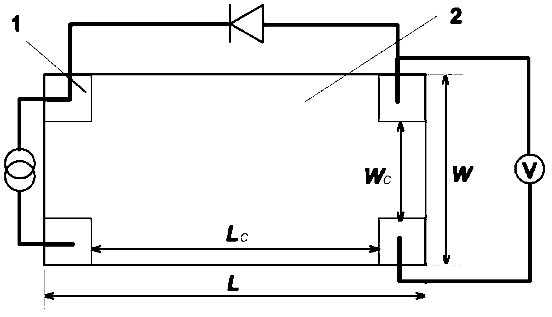
[0029] Set the resistivity to 10 7 The Ω?cm semi-insulating GaAs (100) substrate was rinsed with alcohol or acetone, and cut into a rectangle with a length of L = 7.0 mm and a width of W = 2.3 mm. High-purity soft metal In (purity>99.9%) is used to press the metal electrodes on the four corners of the rectangular GaAs substrate. The size of the metal electrode is 1.0 mm along the length direction of the GaAs substrate and 0.9 mm along the width direction of the GaAs substrate. Therefore L C = 5.0 mm, W C = 0.5 mm. So far, a gallium arsenide-based geometric giant magnetoresistive device has been fabricated.

[0030] When using the four-electrode method to measure the magnetoresistance performance of the device, the current source connected to two adjacent metal electrodes in the width direction provides current, and the voltmeter connected to the other two adjacent metal electrodes in the width direction tests the voltage. A diode is connected between a pair of adjacent...

Embodiment 2

[0034] Set the resistivity to 10 7 The Ω?cm semi-insulating GaAs (100) substrate was rinsed with alcohol or acetone, and cut into a rectangle with a length of L = 4.3 mm and a width of W = 2.3 mm. The electrodes are pressed on the four corners of the rectangular GaAs substrate with high-purity soft metal In (purity>99.9%). The size of the electrodes is 1.15 mm along the length direction of the GaAs substrate and 0.9 mm along the width direction of the GaAs substrate. Therefore L C = 2.0 mm, W C = 0.5 mm. So far, a gallium arsenide-based geometric giant magnetoresistive device has been fabricated.

[0035] The test method, conditions and equipment of the prepared gallium arsenide-based geometric giant magnetoresistor are the same as those in Example 1.

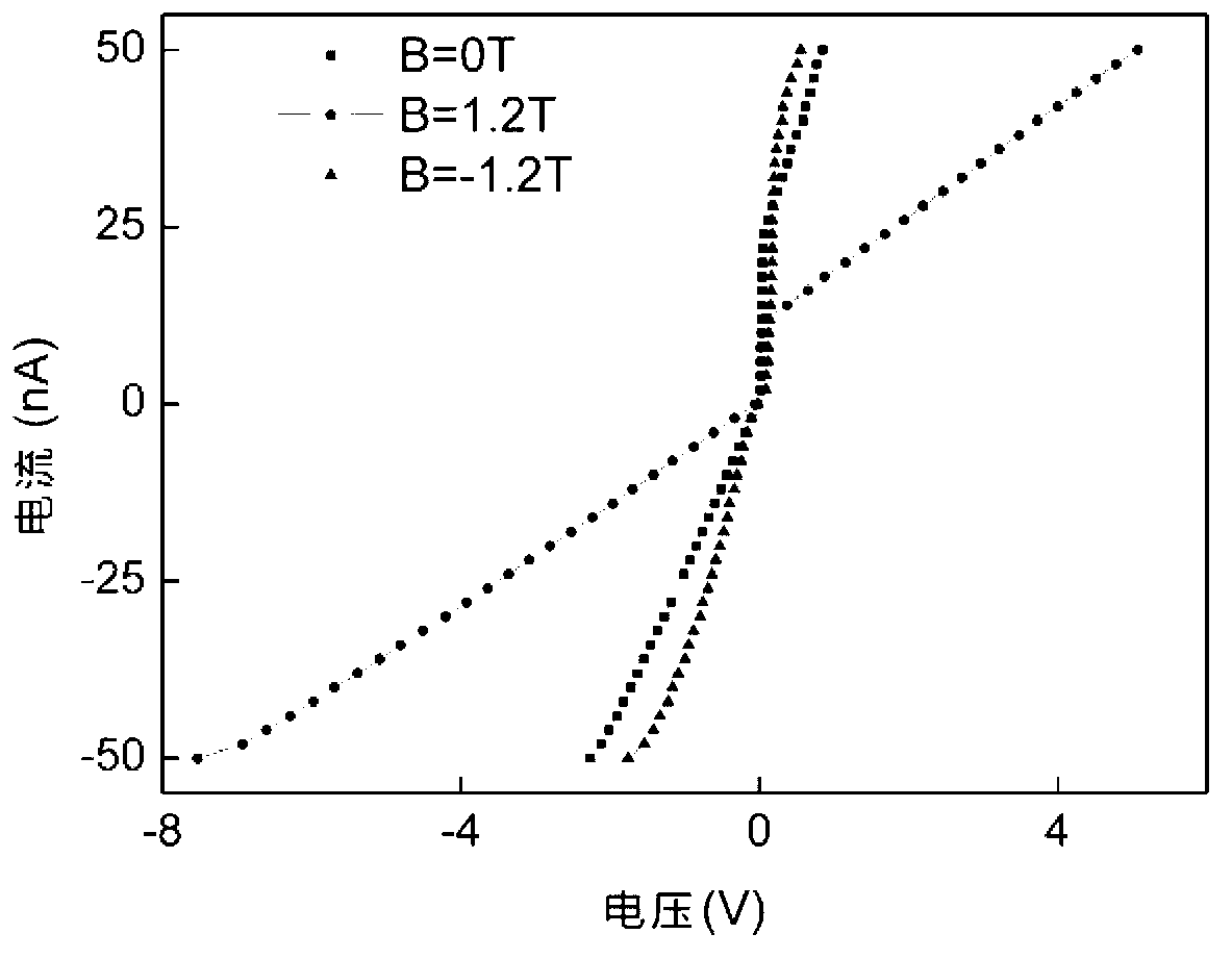
[0036] When the current is 24 nA, its magnetoresistance can reach 700% under the condition of 1.2 T magnetic field.

Embodiment 3

[0038] Set the resistivity to 10 7 The Ω?cm semi-insulating GaAs (100) substrate was rinsed with alcohol or acetone, and cut into a rectangle with a length of L = 4.3 mm and a width of W = 2.3 mm. The electrodes are pressed on the four corners of the rectangular GaAs substrate with high-purity soft metal In (purity>99.9%). The size of the electrodes is 1.15 mm along the length direction of the GaAs substrate and 0.9 mm along the width direction of the GaAs substrate. Therefore L C = 2.0 mm, W C = 0.5 mm. So far, a gallium arsenide-based geometric giant magnetoresistive device has been fabricated.

[0039] The prepared gallium arsenide-based geometric giant magnetoresistor uses a Zener diode with a reverse breakdown voltage of 15V, and its test method, conditions and equipment are the same as those in Example 1.

[0040] When the current is 24 nA, its magnetoresistance can reach 1000% under the condition of 1.2 T magnetic field.


PUM

PropertyMeasurementUnit
lengthaaaaaaaaaa
electrical resistivityaaaaaaaaaa
lengthaaaaaaaaaa

Abstract

The invention belongs to the technical field of magnetic field detection, magnetic field sensor materials and devices, and particularly relates to a gallium arsenide-based geometrical giant magnetoresistance device and a preparation method of the gallium arsenide-based geometrical giant magnetoresistance device. The gallium arsenide-based geometrical giant magnetoresistance device is provided with a metal electrode on each of the four corners of the surface of a rectangular monocrystal GaAs (100) or rectangular monocrystal GaAs (111) substrate, and four metal electrodes are in a rectangular or trapezoidal shape. The preparation method of the gallium arsenide-based geometrical giant magnetoresistance device comprises the following steps of: after cleanly rinsing the GaAs substrate by using alcohol or acetone, clipping the GaAs substrate into a rectangular shape, respectively depositing or pressing high-purity soft metal into metal electrodes on the four corners of the rectangular monocrystal GaAs substrate, so as to the gallium arsenide-based geometrical giant magnetoresistance device. The obtained gallium arsenide-based geometrical giant magnetoresistance device has an obvious magnetoresistance effect, and the magnetoresistance of the device is more than the magnetoresistance of the conventional GaAs-based magnetoresistance device. The obtained gallium arsenide-based geometrical giant magnetoresistance device has the advantages of simple structure, moderate price of raw materials, simple preparation process and environmental friendliness.

Description

technical field [0001] The invention belongs to the technical field of magnetic field detection and magnetic field sensor materials and devices, and in particular relates to a gallium arsenide-based geometric giant magnetoresistance device and a preparation method thereof. Background technique [0002] Since A. Fert and Peter Grünberg (Phys. Rev. Lett. 61(1988) 2472) discovered the giant magnetoresistance effect (GMR) in Fe / Cr multilayer film in 1988, the application of this effect has brought people's life a huge innovation. GMR and the similar tunnel magnetoresistance effect (TMR) are widely used in computer storage technology, high-sensitivity magnetic sensors and space technology and other fields. However, their main raw materials are magnetic metal materials and rare earth materials. With the continuous shortage of rare earth resources, looking for new materials has become a trend. With the development of spintronics, it is found that the magnetoresistance effect als...

Claims


Application Information

Patent Timeline
Patent Type & Authority Applications(China)
IPC IPC(8): H01L43/08H01L43/12H10N50/10H10N50/01
Inventor 章晓中王集敏万蔡华朴红光
Owner TSINGHUA UNIV
Learn More