Wide-band gap multi-heterojunction tunnel junction structure
A multi-heterojunction and tunneling junction technology, which is applied in the field of wide-bandgap multi-heterojunction tunneling junction structures, can solve the problems of low peak current density of wide-bandgap tunneling junctions, etc. The effect of resistance
- Summary
- Abstract
- Description
- Claims
- Application Information
AI Technical Summary
Problems solved by technology
Method used
Image
Examples
Embodiment Construction
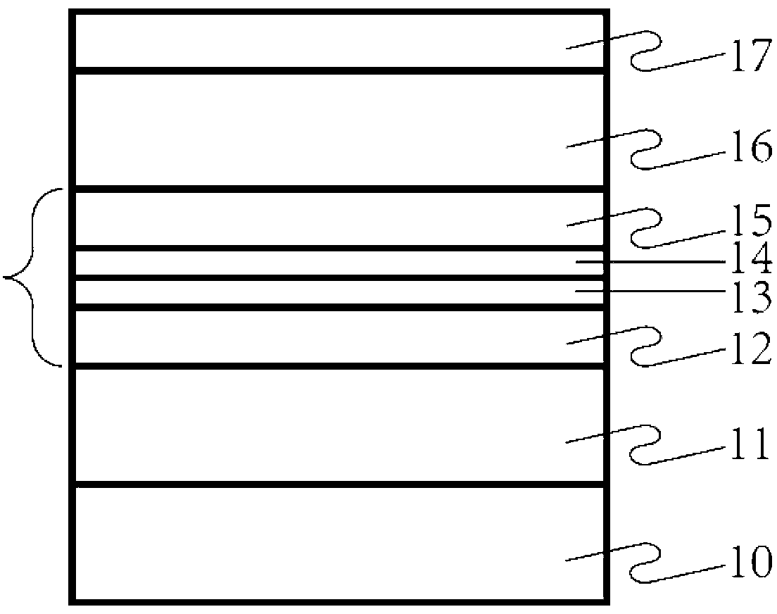
[0014] The first embodiment of the present invention is as figure 1 As shown, there are first bandgap subcell 11, first functional layer 12, second functional layer 13, third functional layer 14, fourth functional layer 15, second bandgap subcell 16 and hat layer 17. The substrate 10 is Ge or GaAs. The first bandgap subcell 11 is a PN-type homojunction or heterojunction composed of one or more materials such as GaAs, GaInAs, GaInNAs, GaInNAsSb, GaInAsP, AlGaAs, AlGaAsP, AlGaInAs, GaInP, AlGaInP. The first functional layer 12 is made of AlGaInP, the Al composition is 0.85, doped with Si, the thickness is 20-100nm, and the doping concentration is 1×10 19 cm -3 ; The second functional layer 13 is made of AlGaInP, the Al composition is 0.15, the doping is Si, the thickness is 10-20nm, and the doping concentration is 5×10 19 cm -3 ; The third functional layer 14 is composed of AlGaAs, the Al composition is 0.15, the doping is C, the thickness is 10-20nm, and the doping concent...
PUM
 Abstract
Description
Claims
Application Information
 - R&D
- Intellectual Property
- Life Sciences
- Materials
- Tech Scout
- Unparalleled Data Quality
- Higher Quality Content
- 60% Fewer Hallucinations
Browse by: Latest US Patents, China's latest patents, Technical Efficacy Thesaurus, Application Domain, Technology Topic, Popular Technical Reports.
© 2025 PatSnap. All rights reserved.Legal|Privacy policy|Modern Slavery Act Transparency Statement|Sitemap|About US| Contact US: help@patsnap.com


