Preparation method of ZnO-based scintillating thick film
A thick film and powder technology, applied in the field of preparation of inorganic scintillation materials, can solve the problems of high mismatch between sapphire substrate and ZnO, poor crystalline quality of thick film, etc., and achieves a small volume, convenient preparation and low growth cost. Effect
- Summary
- Abstract
- Description
- Claims
- Application Information
AI Technical Summary
Problems solved by technology
Method used
Image
Examples
Embodiment 1
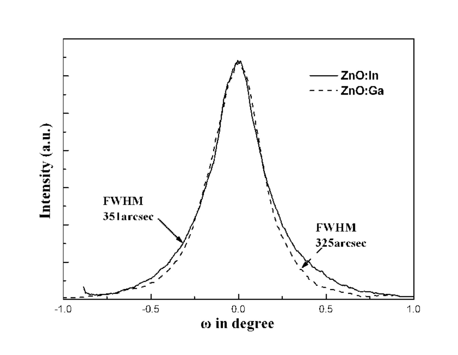
[0030]By adopting the technical scheme of the present invention, a 3mm thick 6H-sapphire single crystal is used as a substrate material to prepare a high crystal quality ZnO:In scintillation thick film. The whole process is divided into three steps:
[0031] 1. Target production
[0032] Use the preparation method of the ZnO-based ceramic target material in the content of the present invention above to prepare ZnO:In target material, In mixed powder 2 o 3 The doping concentration was 0.35wt%, the sintering temperature was 1300°C, and the time was 12 hours. After the sintering was completed, it was polished according to the normal process, washed with alcohol and pure water three times, and placed in a magnetically bound inductively coupled physical sputtering apparatus for pre-sputtering to form sputtering tracks.
[0033] 2. thin film deposition
[0034] A 3mm 6H-sapphire single wafer with good crystal quality is selected as the substrate material, and both sides are req...
Embodiment 2
[0040] By adopting the technical scheme of the present invention, a 0.4mm thick 6H-sapphire single crystal is used as a substrate material to prepare a high crystal quality ZnO:Ga scintillation thick film. The whole process is divided into three steps:
[0041] 1. Target production
[0042] Use the preparation method of the ZnO-based ceramic target material in the content of the present invention to prepare ZnO:Ga target material, Ga in the mixed powder 2 o 3 The doping concentration was 0.15wt%, the temperature was 950°C, and the time was 8 hours. After the sintering was completed, it was polished according to the normal process, washed with alcohol and pure water three times, and placed in a magnetically bound inductively coupled physical sputtering apparatus for pre-sputtering to form sputtering tracks.
[0043] 2. thin film deposition
[0044] A 0.4mm 6H-sapphire single wafer with good crystal quality is selected as the substrate material, and both sides are required ...
PUM
| Property | Measurement | Unit |
|---|---|---|
| size | aaaaa | aaaaa |
| thickness | aaaaa | aaaaa |
| thickness | aaaaa | aaaaa |
Abstract
Description
Claims
Application Information
 - Generate Ideas
- Intellectual Property
- Life Sciences
- Materials
- Tech Scout
- Unparalleled Data Quality
- Higher Quality Content
- 60% Fewer Hallucinations
Browse by: Latest US Patents, China's latest patents, Technical Efficacy Thesaurus, Application Domain, Technology Topic, Popular Technical Reports.
© 2025 PatSnap. All rights reserved.Legal|Privacy policy|Modern Slavery Act Transparency Statement|Sitemap|About US| Contact US: help@patsnap.com


