
Ultra-low-power organic resistance changing memory device and manufacturing method thereof

A technology of resistive variable memory and ultra-low power consumption, which is applied in the field of ultra-low power organic resistive variable memory devices and its preparation, can solve problems hindering the development and application of organic resistive variable memory, and save preparation time, programming and erasing In addition to the effect of small current and good compatibility

Active Publication Date: 2012-07-25
SEMICON MFG INT (SHANGHAI) CORP +1
View PDF5 Cites 13 Cited by
  • Summary
  • Abstract
  • Description
  • Claims
  • Application Information

AI Technical Summary

Problems solved by technology

However, there has never been a report on the realization of ultra-low power consumption of organic resistive memory. High power consumption has hindered the development and application of organic resistive memory to a large extent.

Method used


Image

  • Ultra-low-power organic resistance changing memory device and manufacturing method thereof
  • Ultra-low-power organic resistance changing memory device and manufacturing method thereof
  • Ultra-low-power organic resistance changing memory device and manufacturing method thereof

Examples


Embodiment Construction

[0024] Below in conjunction with accompanying drawing, the present invention is described in further detail by specific embodiment:

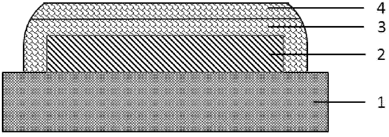
[0025] The process flow of the present invention for preparing ultra-low power organic resistive variable memory is as follows: Figure 1-Figure 5 as shown,

[0026] 1) Utilize physical vapor deposition (PVD) method or other film-forming methods in the integrated circuit (IC) process to form a metal Pt film on the silicon substrate 1, with a thickness between 100nm and 400nm, and use standard photolithography technology to make Its electrodes are patterned to prepare the bottom electrode 2, such as figure 1 shown;

[0027] 2) Utilize Polymer CVD technology to grow the first layer of C-type parylene-C (Parylene-C) film 3, such as figure 2 shown. Then, adopt the same method to deposit one deck of C-type parylene film 4 again on the first layer of C-type parylene, as image 3 shown. Polymer CVD equipment is used for deposition, and the stand...


PUM

PropertyMeasurementUnit
Thicknessaaaaaaaaaa
Thicknessaaaaaaaaaa

Abstract

The invention discloses an ultra-low-power organic resistance changing memory device and a manufacturing method of the ultra-low-power organic resistance changing memory device, belonging to the technical field of organic electronics and CMOS-mixed integrated circuit. The device is manufactured on a substrate, a device unit is an MIM capacity structure, a bottom layer of the MIM structure is an inert electrode such as metal or non-metal conductive thin-film, a top layer of the MIM structure is an active electrode such as metal Al, a middle function layer of the MIM sturcture is a poly-p-xylylene polymer film growing after multi-deposition. According to the invention, the device adopts the poly-p-xylylene polymer film growing after multi-deposition as the function layer, programming current of a memory is less than 0.5 muA, and erase current of the memory is reduced to about 10 nA or lower, therefore, the ultra-low-power operations of the organic resistance changing memory are implemented.

Description

technical field [0001] The invention belongs to the technical fields of organic electronics and CMOS hybrid integrated circuits, and in particular relates to an ultra-low power consumption organic resistance variable memory device and a preparation method thereof. Background technique [0002] As integrated circuits and computer systems are becoming more complex, power consumption is a growing concern. Memory is an essential component in circuits and systems, and its power consumption has become more and more important in design. At present, the non-volatile memory on the market is mainly based on flash memory (flash memory). However, as the technology nodes of integrated circuits continue to advance, flash memory technology will reach its physical limit and cannot meet the needs of miniaturization and low power consumption of electronic devices. need. Therefore, in recent years, a new generation of storage technology represented by resistive variable memory has become a r...

Claims


Application Information

Patent Timeline
IPC IPC(8): H01L51/00G11C13/00
Inventor 黄如白文亮蔡一茂唐昱张兴
Owner SEMICON MFG INT (SHANGHAI) CORP
Learn More