
Micro-voltage high-overload sensor chip of beam membrane single island structure

A sensor chip, high overload technology, applied in the direction of microstructure technology, microstructure devices, piezoelectric devices/electrostrictive devices, etc., can solve problems such as staying, not being able to adapt to the working environment in the aerospace field, and not being able to meet the precise measurement requirements in the aerospace field

Inactive Publication Date: 2012-07-18
XI AN JIAOTONG UNIV
View PDF7 Cites 26 Cited by
  • Summary
  • Abstract
  • Description
  • Claims
  • Application Information

AI Technical Summary

Problems solved by technology

[0003] With the development of aerospace technology, my country's current MEMS micro-pressure sensors are still mainly at the KPa level, which cannot meet the needs of the aerospace field for Pa-level micro-pressure measurement, nor can it adapt to the working environment of the aerospace field, and cannot meet the needs of the aerospace field. Requirements for precise measurement technology of deep and high-altitude micro-pressure

Method used


Image

  • Micro-voltage high-overload sensor chip of beam membrane single island structure
  • Micro-voltage high-overload sensor chip of beam membrane single island structure
  • Micro-voltage high-overload sensor chip of beam membrane single island structure

Examples


Embodiment Construction

[0020] Embodiments of the present invention will be described in detail below with reference to the accompanying drawings.

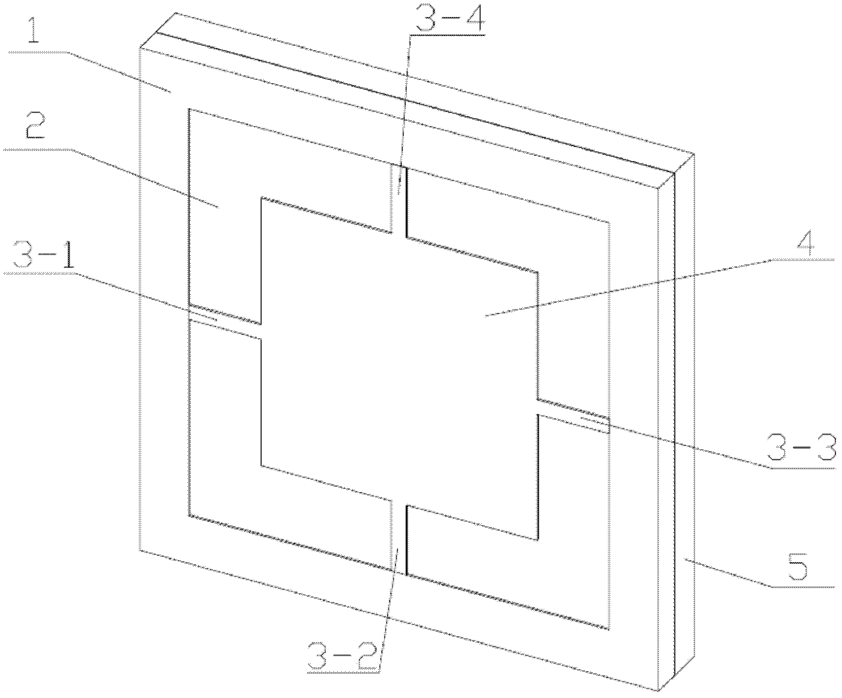
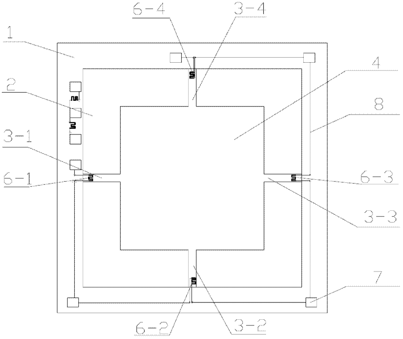
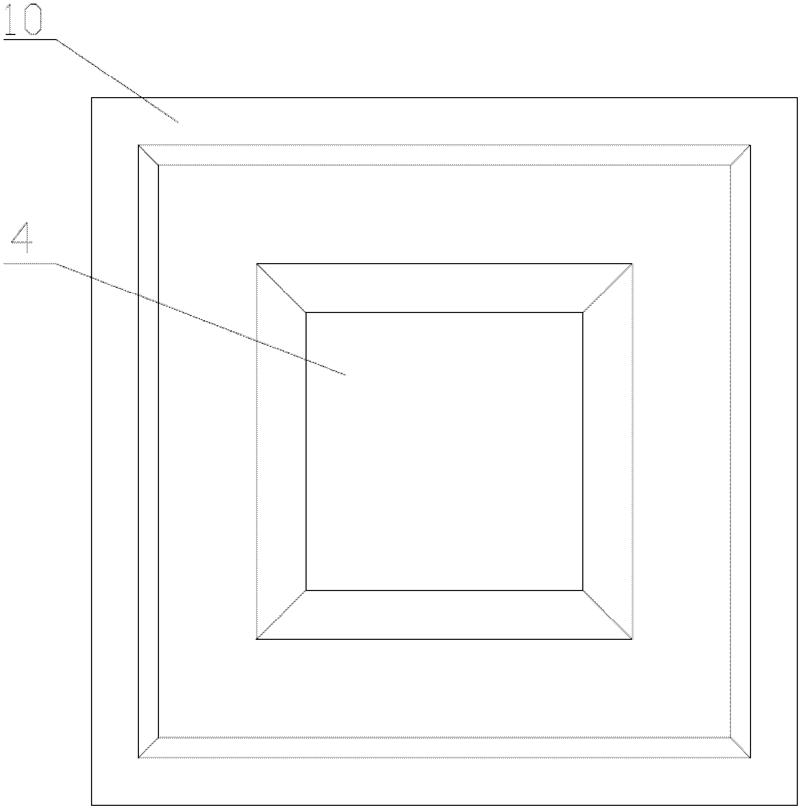
[0021] refer to figure 1 and figure 2 , a beam-membrane single-island structure micro-pressure high overload sensor chip, comprising a silicon substrate 1, and a mass block 4 and four single beams 3-1, 3-2, 3-3, 3-4 are processed in the middle of the silicon substrate 1 , the mass block 4 is connected to the silicon substrate 1 through four single beams 3-1, 3-2, 3-3, 3-4, and the silicon substrate 1, the mass block 4 and the four single beams 3-1, 3-2 are connected , 3-3, 3-4 are processed into a thin film 2 with a thickness of 10-30 μm, the back of the silicon substrate 1 is bonded with the Pyrex7740 glass 5, and the back of the mass 4 is thinned to make the mass 4 and Pyrex7740 glass 5 Leave a gap of 5-10μm in the vacuum environment, refer to image 3 and Figure 4 , insert the anti-adsorption electrode 9 on the Pyrex7740 glass 5 into the bonding...


PUM

PropertyMeasurementUnit
thicknessaaaaaaaaaa

Abstract

The invention provides a micro-voltage high-overload sensor chip of a beam membrane single island structure, comprising a silicon base, wherein a mass block and four single beams are machined at the middle part of the silicon base; a thin film with the thickness of 10-30 mu m is machined in a space surrounded by the silicon base, the mass block and the four single beams; the back side of the silicon base is bonded with Pyrex7740 glass and a gap of 5-10 mu m is reserved between the mass block and the Pyrex7740 glass under a vacuum environment by thinning the back side of the mass block; meanwhile, an anti-adsorbing electrode on the Pyrex7740 glass is inserted into a bonding region and a cavity formed among the thin film, the mass block and the Pyrex7740 glass is vacuumized; and at the front side of the silicon base, four piezoresistor strips are mutually connected to form a semi-open-loop Wheatstone bridge. The four piezoresistor strips are introduced to improve the rigidity of the whole body and the stress is concentrated again; the micro-voltage high-overload sensor chip has the characteristics of good linearity and high flexibility; and meanwhile, the micro-voltage high-overload sensor chip can resist 500 times of high overload.

Description

technical field [0001] The invention relates to the technical field of MEMS piezoresistive absolute pressure sensors, in particular to a beam-membrane single-island structure micro-pressure high-overload sensor chip. Background technique [0002] With the development of micro-mechanical electronic system technology, MEMS micro-pressure sensors have been widely used in wind tunnel testing, biomedical electronics and petrochemical fields, especially in aerospace, which has strict requirements on the size and weight of sensors, MEMS The sensor is undoubtedly a very ideal choice. [0003] With the development of aerospace technology, my country's current MEMS micro-pressure sensors are still mainly at the KPa level, which cannot meet the needs of the aerospace field for Pa-level micro-pressure measurement, nor can they adapt to the working environment in the aerospace field, and cannot meet the needs of the aerospace field. The demand for precise measurement technology of deep a...

Claims


Application Information

Patent Timeline
Patent Type & Authority Applications(China)
IPC IPC(8): G01L1/18B81B3/00B81B7/02
Inventor 赵玉龙于忠亮孟夏薇田边王伟忠
Owner XI AN JIAOTONG UNIV
Learn More