Composite back-reflective metal electrode for thin film solar cell, preparation method and application thereof
A technology of thin-film solar cells and metal electrodes, which is applied in the manufacture of circuits, electrical components, and final products. It can solve the problems of easy falling off, low adhesion between the back reflector and the substrate, etc., so that it is not easy to fall off and ensures texture effect, the effect of relieving interfacial stress
- Summary
- Abstract
- Description
- Claims
- Application Information
AI Technical Summary
Problems solved by technology
Method used
Image
Examples
Embodiment 1
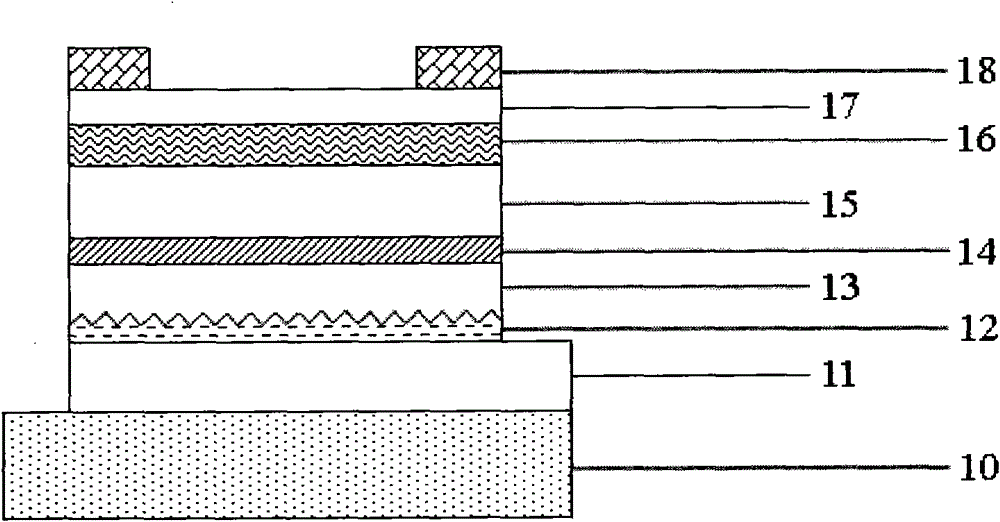
[0030] figure 1 A schematic diagram of the structure of a single-junction silicon-based thin-film solar cell comprising a composite back-reflecting metal electrode of the present invention is provided. According to the present invention, the main steps of preparing the main body of the solar cell are as follows:
[0031] The first step: put the prepared substrate containing the metal transition layer (nickel or cadmium or copper or titanium), the textured silver film, and the aluminum-doped zinc oxide barrier layer into the plasma-enhanced chemical vapor deposition system, the substrate Bake at 200°C for 1 hour;
[0032] The second step: sequentially deposit n, i, p three layers of silicon-based films in different chambers;
[0033] Step 3: Cool down to room temperature, take out the sample; place the sample prepared with silicon-based thin film in the coating system, and prepare aluminum-doped zinc oxide, tin dioxide or indium tin oxide transparent conductive film;
[0034]...
Embodiment 2
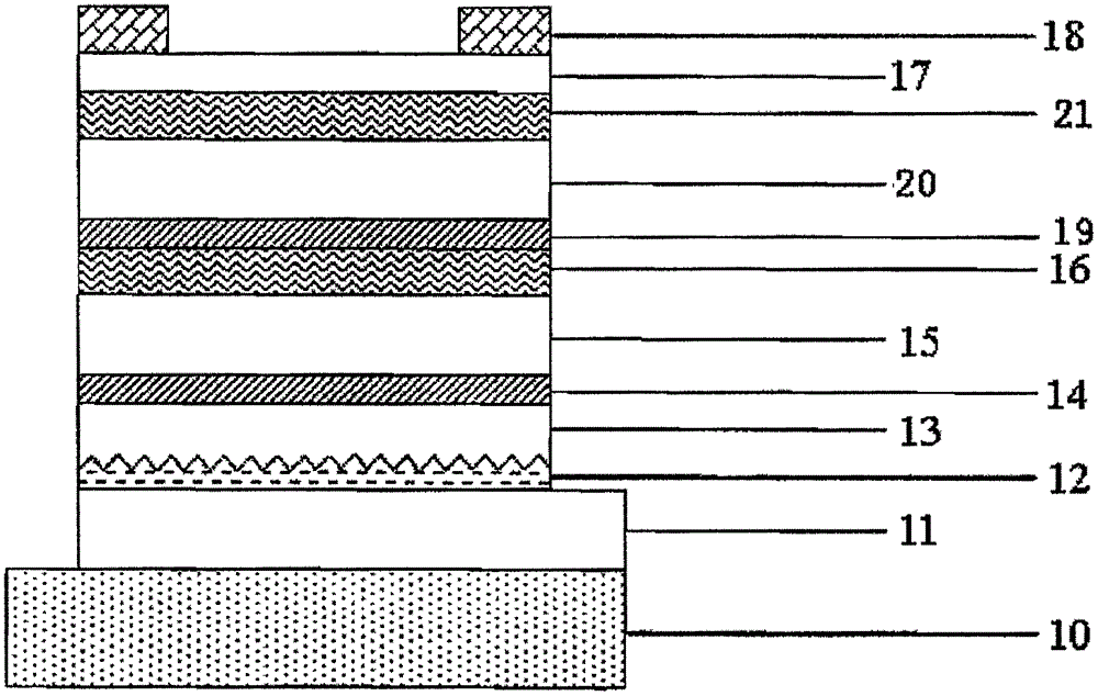
[0038] image 3 A schematic structural view of a multi-junction silicon-based thin-film solar cell comprising a composite back-reflecting metal electrode of the present invention is provided. According to the present invention, the main steps of preparing the solar cell body are as follows:
[0039] The first step: put the prepared substrate containing the metal transition layer (nickel or cadmium or copper or titanium), the textured silver film, and the aluminum-doped zinc oxide barrier layer into the plasma-enhanced chemical vapor deposition system, the substrate Bake at 200°C for 1 hour;
[0040] The second step: sequentially deposit n, i, p three layers of silicon-based films 14-16 in different chambers;
[0041] The third step: sequentially deposit n, i, p three layers of silicon-based films 19-21 in different chambers;
[0042] Step 4: Cool down to room temperature, take out the sample; place the sample prepared with silicon-based thin film in the coating system, and pre...
PUM
| Property | Measurement | Unit |
|---|---|---|
| thickness | aaaaa | aaaaa |
| thickness | aaaaa | aaaaa |
| thickness | aaaaa | aaaaa |
Abstract
Description
Claims
Application Information
 - Generate Ideas
- Intellectual Property
- Life Sciences
- Materials
- Tech Scout
- Unparalleled Data Quality
- Higher Quality Content
- 60% Fewer Hallucinations
Browse by: Latest US Patents, China's latest patents, Technical Efficacy Thesaurus, Application Domain, Technology Topic, Popular Technical Reports.
© 2025 PatSnap. All rights reserved.Legal|Privacy policy|Modern Slavery Act Transparency Statement|Sitemap|About US| Contact US: help@patsnap.com


