Layer-by-layer analysis method for surface layer of copper alloy material
An analysis method and technology for copper alloys, applied in the field of layer-by-layer analysis of the surface of alloy materials
- Summary
- Abstract
- Description
- Claims
- Application Information
AI Technical Summary
Problems solved by technology
Method used
Image
Examples
Embodiment 1
[0036] The method of layer-by-layer analysis on the surface of copper alloy materials by glow discharge mass spectrometry includes the following steps:
[0037] (1) Prepare samples for analysis
[0038] Grind an unknown commercially available brass substrate to 9. It is further polished to a mirror surface, and a thin aluminum bronze film is grown on the substrate surface by radio frequency sputtering deposition; first, the thickness of the aluminum bronze film is calibrated by scanning electron microscope analysis technology, and its thickness is 5.0 μm;
[0039] (2) Select the analysis conditions of the instrument
[0040] Glow discharge ion source conditions: the sampling distance is 12mm, the sample sputtering spot diameter is φ5mm, the ion source argon pressure is 800Pa, and the discharge voltage is DC 800V;
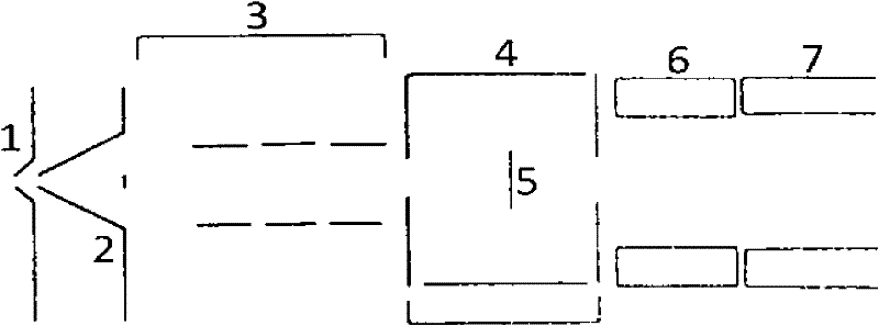
[0041] Glow discharge ion source mass spectrometry interface conditions: the aperture of the ion outlet cone 1 is φ6mm, the aperture of the intercepting cone 2 is φ0.89mm, ...
PUM
| Property | Measurement | Unit |
|---|---|---|
| thickness | aaaaa | aaaaa |
Abstract
Description
Claims
Application Information
 - Generate Ideas
- Intellectual Property
- Life Sciences
- Materials
- Tech Scout
- Unparalleled Data Quality
- Higher Quality Content
- 60% Fewer Hallucinations
Browse by: Latest US Patents, China's latest patents, Technical Efficacy Thesaurus, Application Domain, Technology Topic, Popular Technical Reports.
© 2025 PatSnap. All rights reserved.Legal|Privacy policy|Modern Slavery Act Transparency Statement|Sitemap|About US| Contact US: help@patsnap.com


