
Quenching and reading circuit for single photon avalanche diode imaging device

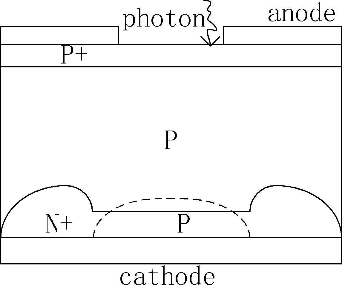
A single-photon avalanche and readout circuit technology, applied in televisions, electrical components, color televisions, etc., can solve the problems of occupied area, large area, and large occupation, and achieve high detection accuracy, improved integration, and high detection sensitivity Effect

Active Publication Date: 2014-05-07
NANJING UNIV OF POSTS & TELECOMM INST AT NANJING CO LTD
View PDF3 Cites 0 Cited by
  • Summary
  • Abstract
  • Description
  • Claims
  • Application Information

AI Technical Summary

Problems solved by technology

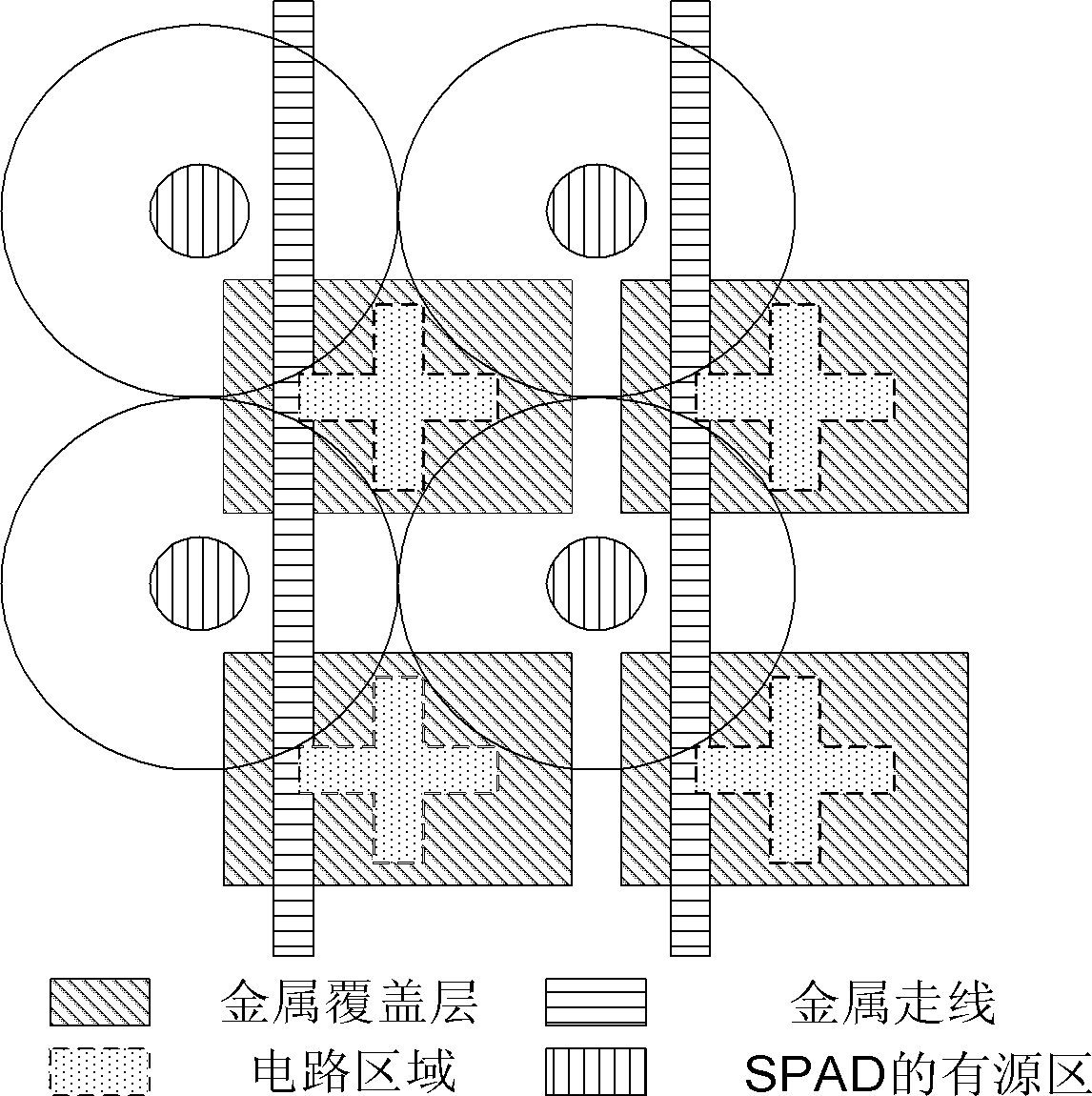
It can be inferred that a SPAD system needs to use a digital counter connected to an APD, and if it is expanded, it will also use chips such as address decoders, because the APD device itself is larger than the general quenching and readout circuit and occupies a larger area, such as image 3 , so the cost of this method is too high, coupled with the peripheral counter decoder, etc., it obviously takes up too much area

Method used


Image

  • Quenching and reading circuit for single photon avalanche diode imaging device
  • Quenching and reading circuit for single photon avalanche diode imaging device
  • Quenching and reading circuit for single photon avalanche diode imaging device

Examples


Embodiment

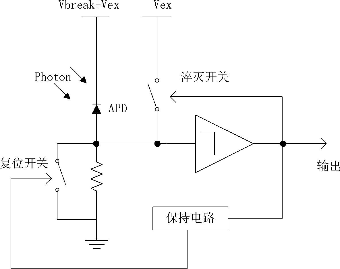
[0056] Based on the smic 0.13um nor flash process, the circuit of the present invention has been simulated and verified. In order to ensure the accuracy of the simulation results, the avalanche diode is used Figure 6 The circuit model shown is replaced, and the parameters of the circuit model are shown in Table 1.

[0057] Table 1 Model parameters

[0058]

[0059] Parameter Physical Definition Value

[0060]

[0061] C0 The capacitance between the cathode (cathode) and the anode (anode) 500fF

[0062] C1 Capacitance between cathode and substrate 500fF

[0063] C2 Anode (anode) capacitance between substrates 500fF

[0064] R S The off resistance of the diode in the steady state is 250ohm

[0065] Vbreak Diode Avalanche Threshold Voltage 12V

[0066] T Simulated photon energy generation can cause diode avalanche to close—2.5V

[0067] disconnect-...


PUM


Abstract

The invention aims at providing a quenching and reading circuit for a single photon avalanche diode imaging device, which is composed of three modules including a quenching circuit, a holding circuit and a reading circuit, wherein the quenching circuit is used for generating a pulse signal having the same frequency with an incident photon signal, the holding circuit is used for generating a reset signal, the phase of the reset signal is different from the phase of quenching output, the frequency of the reset signal is the same with the frequency of the quenching output, and the reading circuit is used for performing count processing on the quenching output pulse signal and outputting the signal in a linear and logarithmic mode. Quenching processing is performed on an avalanche diode after photon incidence by utilizing the quenching circuit, pulse signal output with the same frequency as incident photons is generated and directly sent into the reading circuit, the reading circuit selects to output a final result in a linear or a logarithmic mode according to the control of a plus signal, and simultaneously the quenching output pulse is delayed to keep the frequency unchanged and the phase changed to serve as the reset signal for controlling the staring or stopping of quenching.

Description

technical field [0001] The invention relates to a quenching and readout circuit of a single photon avalanche diode imaging device. The circuit can quickly realize the quenching of large avalanche current and the accurate counting of incident photons. The overall circuit integration is high, it has extremely high detection sensitivity, and the output dynamic range is wide. It can be directly used in the existing mature CMOS APS imaging device. The architecture constructs a large-scale array, which greatly improves the resolution of the device. Background technique [0002] In recent decades, the traditional imaging technology based on Charge Coupled Device (CCD, Charge Coupled Device) and CMOS Active Pixel Image Sensor (CMOS APS, Active Pixel Sensor) has made great progress, but with the development of quantum information technology With the development, the imaging speed and pixel sensitivity of traditional imaging technology have encountered great challenges. More and mor...

Claims


Application Information

Patent Timeline
Patent Type & Authority Patents(China)
IPC IPC(8): H04N5/374H04N5/378
Inventor 徐跃赵菲菲吴金山王凱玄何迟
Owner NANJING UNIV OF POSTS & TELECOMM INST AT NANJING CO LTD
Learn More