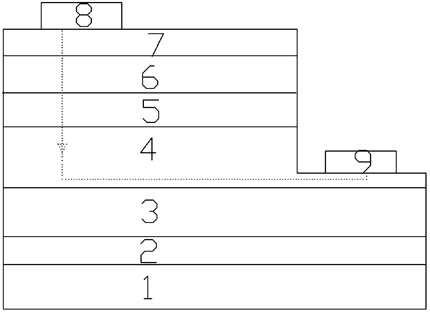
LED (light-emitting diode) epitaxial wafer
An LED epitaxial wafer and epitaxial wafer technology, applied in electrical components, circuits, semiconductor devices, etc., can solve the problems of low light output efficiency, short service life, uneven current expansion, etc., to improve luminous efficiency, improve injection efficiency, structure simple effect
- Summary
- Abstract
- Description
- Claims
- Application Information
AI Technical Summary
Problems solved by technology
Method used
Image
Examples
preparation example Construction
[0031] The preparation method of LED epitaxial wafer comprises the following steps:
[0032] (1) In the MOCVD reaction chamber, put crystal form Heating the sapphire substrate 1 on the (0001) plane, removing surface H under a hydrogen atmosphere 2 O and O 2 ;
[0033] (2) growing gallium nitride nucleation layer 2 according to a conventional method;
[0034] (3) growing an unintentionally doped gallium nitride buffer layer 3 by a conventional method;
[0035] (4) Growth of Al by conventional methods x Ga 1-x N(0.2y al 1-y Insertion layer 3 of N (018 cm -3 .
[0036] (5) The N-type gallium nitride layer 4 is grown according to a conventional method, and the doping element is Si atoms.
[0037] (6) On the N-type gallium nitride layer 4, grow quantum well layers / barrier layers 5 of n periods (n is an integer) by conventional methods;
[0038] (7) grow the P-type gallium nitride layer 6 according to a conventional method, and dope Mg atoms in the P-type gallium nitride ...
PUM
 Abstract
Description
Claims
Application Information
 - Generate Ideas
- Intellectual Property
- Life Sciences
- Materials
- Tech Scout
- Unparalleled Data Quality
- Higher Quality Content
- 60% Fewer Hallucinations
Browse by: Latest US Patents, China's latest patents, Technical Efficacy Thesaurus, Application Domain, Technology Topic, Popular Technical Reports.
© 2025 PatSnap. All rights reserved.Legal|Privacy policy|Modern Slavery Act Transparency Statement|Sitemap|About US| Contact US: help@patsnap.com


