Apparatus and method of MBE isoepitaxial growth SrTiO3 film
A homoepitaxy, thin film technology, applied in the direction of single crystal growth, crystal growth, single crystal growth, etc., can solve the problems of insufficient chemical ratio precision of thin film materials, deviation of thin film composition, sample differences, etc., to eliminate sample differences, improve Sensitivity, the effect of improving efficiency
- Summary
- Abstract
- Description
- Claims
- Application Information
AI Technical Summary
Problems solved by technology
Method used
Image
Examples
Embodiment 1
[0034] This embodiment provides a MBE homoepitaxial growth SrTiO 3 Thin film methods, including:
[0035] 1) Processing substrate: choose common commercially available SrTiO 3 The (110) substrate was used as the substrate, sputtered with Ar ions at a sputtering dose of 500eV / 2.0μA / 10min, and then annealed in an ultra-high vacuum at 1000°C to obtain SrTiO with a single-phase (4×1) reconstruction 3 (110) surface, which is the SrTiO cut-off surface;
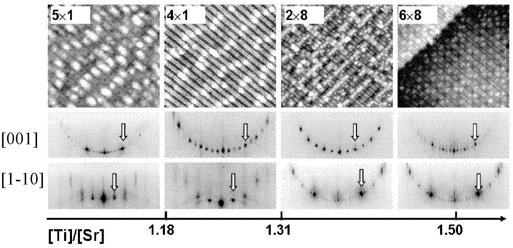
[0036] 2) SrTiO3 (110) Film preparation: Heating the substrate to 800°C, co-depositing Ti and Sr in an oxygen atmosphere, and at the same time performing in-situ real-time monitoring of the sample by reflection high-energy electron diffraction, selecting the [001] direction corresponding to (4×1 ) of the (01) spots of the reconstructed diffraction fringes (such as figure 1 The arrows in the reflective high-energy electron diffraction patterns in the second row and second column of ) are used as characteristic diffraction fringes,...
Embodiment 2
[0044] This embodiment provides a MBE homoepitaxial growth SrTiO 3 Thin film methods, including:
[0045] 1) Processing substrate: choose common commercially available SrTiO 3 The (110) substrate was used as the substrate, sputtered with Ar ions at a sputtering dose of 500eV / 2.0μA / 10min, and then annealed in an ultra-high vacuum at 1000°C to obtain a single-phase (4×1) restructured SrTiO 3 (110) surface, re-growth 0.15 atomic layer of metal Sr to obtain single-phase (5×1) reconstructed SrTiO 3 (110) surfaces;
[0046] 2) SrTiO 3 (110) Film preparation: Heating the substrate to 800°C, co-depositing Ti and Sr in an oxygen atmosphere, and at the same time performing in-situ real-time monitoring of the sample by reflection high-energy electron diffraction, selecting the [001] direction corresponding to (5×1 ) of the (01) spots of the reconstructed diffraction fringes (such as figure 1 The arrows in the reflective high-energy electron diffraction patterns in the second row and...
Embodiment 3
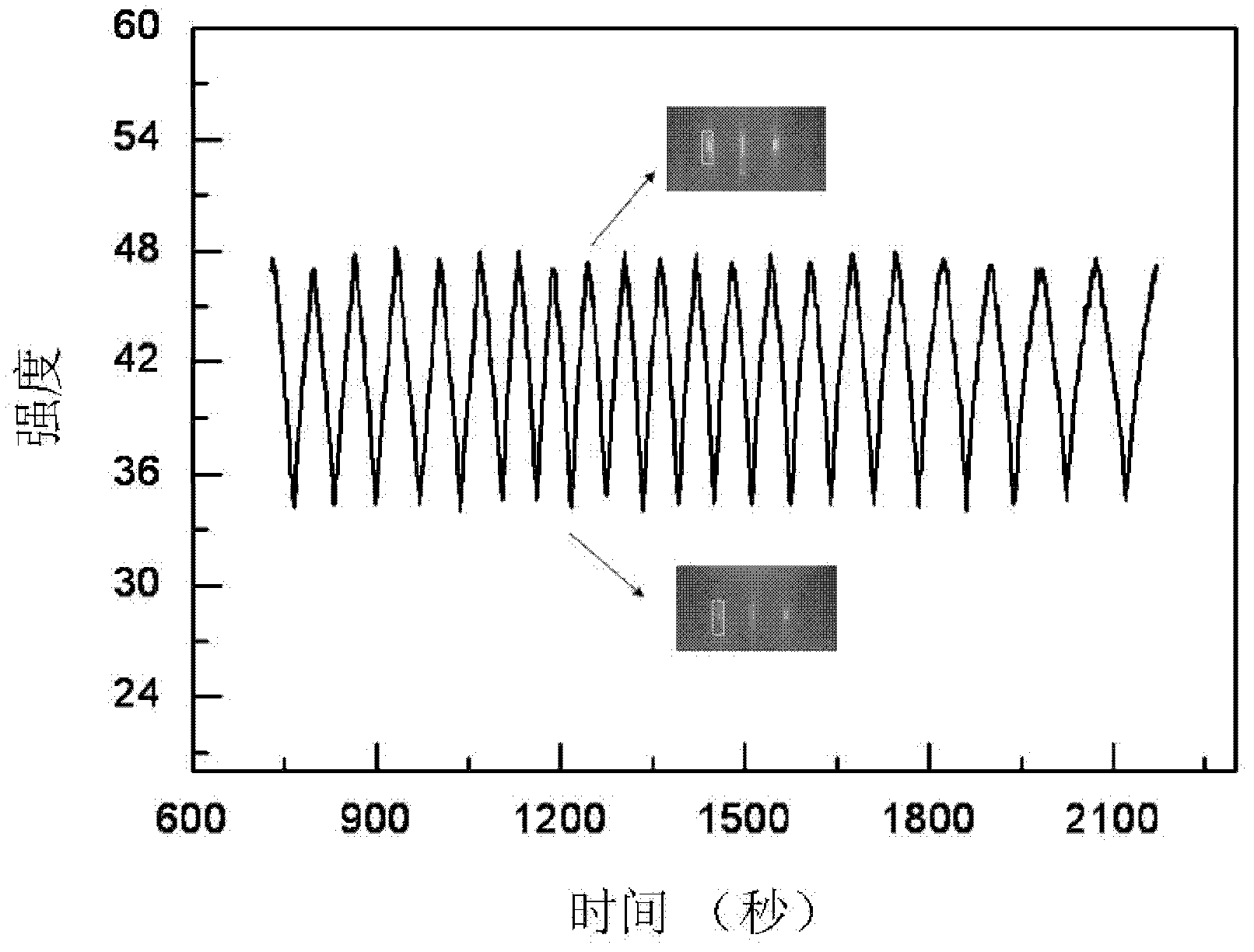
[0054] This embodiment provides a MBE homoepitaxial growth SrTiO 3 thin-film method in SrTiO with single-phase (4 × 1) reconstitution 3 (110) SrTiO growth on substrate surface 3 The thin film is different from the method provided in Example 1 in that an imaging device is used to image the reflective high-energy electron diffraction pattern, and the brightness of the (01) spot of the characteristic diffraction fringe in the [001] direction is monitored in real time, so that the (01) spot Quantification of brightness, and the rest of the growth process is similar to the method provided in Example 1.
[0055] The MBE homoepitaxial growth SrTiO provided in this example 3 Thin film methods include:
[0056] 1) Process the substrate to obtain single-phase (4×1) reconstituted SrTiO 3 (110) substrate surface;
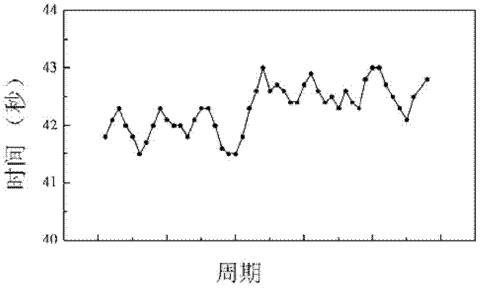
[0057] 2) SrTiO 3 (110) Film preparation: Heating the substrate to 800°C, co-depositing Ti and Sr in an oxygen atmosphere, and at the same time performing in-situ real-ti...
PUM
 Abstract
Description
Claims
Application Information
 - R&D
- Intellectual Property
- Life Sciences
- Materials
- Tech Scout
- Unparalleled Data Quality
- Higher Quality Content
- 60% Fewer Hallucinations
Browse by: Latest US Patents, China's latest patents, Technical Efficacy Thesaurus, Application Domain, Technology Topic, Popular Technical Reports.
© 2025 PatSnap. All rights reserved.Legal|Privacy policy|Modern Slavery Act Transparency Statement|Sitemap|About US| Contact US: help@patsnap.com


