Method for self-assembling micro-electromechanical system (MEMS) based on solder ball laser remelting process

A technology of laser remelting and self-assembly, applied in auxiliary devices, manufacturing tools, metal processing equipment, etc., can solve problems such as inability to deal with complex structures, inapplicability of heating and remelting, complex integration process of solder alloys, etc., and achieve self-assembly The effect of high precision and wide application range

Active Publication Date: 2013-07-31
HARBIN INST OF TECH
View PDF3 Cites 0 Cited by
  • Summary
  • Abstract
  • Description
  • Claims
  • Application Information

AI Technical Summary

Problems solved by technology

[0005] The purpose of the present invention is to provide a MEMS self-assembly method based on the solder ball laser remelting process, to solve the complex integration process of the solder alloy in the existing MEMS self-assembly method based on the surface tension of the molten solder, and the overall heating of the MEMS device. Fusion is not suitable for optical MEMS devices that are sensitive to heat or force, and local heating of resistance to achieve multiple self-assembly processes with a logical sequence. The process is complex and cannot deal with the problem of complex structures.

Method used


Image

  • Method for self-assembling micro-electromechanical system (MEMS) based on solder ball laser remelting process
  • Method for self-assembling micro-electromechanical system (MEMS) based on solder ball laser remelting process
  • Method for self-assembling micro-electromechanical system (MEMS) based on solder ball laser remelting process

Examples


specific Embodiment approach 1

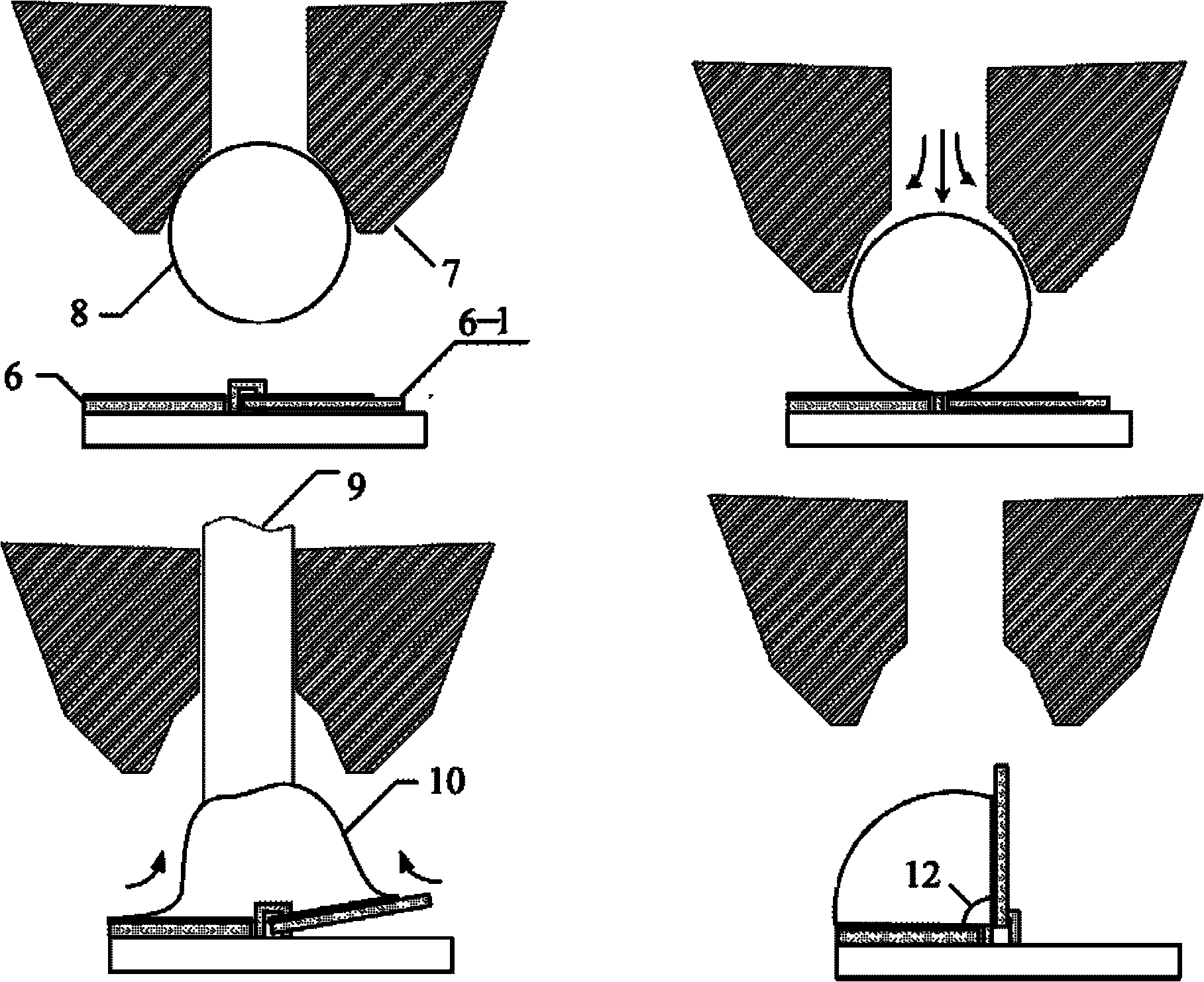
[0020] Specific implementation mode one: combine figure 1 Describe this embodiment, the method of this embodiment comprises the following steps: Step 1: the MEMS chip 6 with self-assembled basic structure that has completed sacrificial layer release is fixed on the clamping device, sucks solder alloy by suction nozzle device 7 ball 8;

[0021] Step 2: the suction nozzle device 7 releases the solder alloy ball 8 in the middle of the connection between the fixed microstructure and the movable microstructure pad on the MEMS chip;

[0022] Step 3: When the solder alloy ball 8 is released, the laser 9 is used to heat and remelt the solder alloy ball 8. After the solder alloy ball 8 is heated to the melting point, the molten solder wets the metal solder on the MEMS chip 6. Disk 6-1, the movable structure of the MEMS chip 6 realizes the turning motion under the action of the surface tension of the molten solder 10;

[0023] Step 4: By controlling the heating time and power of the ...

specific Embodiment approach 2

[0024] Specific embodiment two: the diameter of solder alloy ball 8 in the step 1 of the present embodiment is 200 μ m-400 μ m; 217°C; the power range of the laser used in step 4 is 3-15w, and the laser heating time is 80-800ms. The advantage of this step is that the rapid heating of the laser ensures the self-assembly efficiency. Other steps are the same as in the first embodiment.

specific Embodiment approach 3

[0025] Specific embodiment three: in step three of the present embodiment, the laser beam spot diameter is less than the diameter of the solder alloy ball 8, and only acts on the top of the solder alloy ball 8 to heat it. The advantage of this step is the characteristic of concentrated laser heating It ensures that the chip structure other than the solder ball is not damaged. Other steps are the same as in the first embodiment.


PUM

PropertyMeasurementUnit
diameteraaaaaaaaaa

Abstract

The invention discloses a method for self-assembling a micro-electromechanical system (MEMS) based on a solder ball laser remelting process, and relates to a method for self-assembling the MEMS. The invention aims to solve the problems that: according to the conventional method for self-assembling the MEMS based on the surface tension of molten solders, a process for integrating solder alloys is complicated, the integral heating and remelting of an MEMS device are not applicable to optical MEMS devices which are sensitive to heat and force, and a multiple self-assembly process with a logical sequence which is realized by the local heating of a resistor is complicated and cannot response complicated structures. The scheme 1 is that: a solder ball released on a metal bonding pad of an MEMS chip is heated by laser so as to ensure that the solder ball is molten and pulls a movable structure of the MEMS chip to realize tilting motion. The scheme 2 is that: solder alloy balls are released on a plurality of bonding pad connection centers and are heated and remolten, so that the self-assembly of a first rotating mechanism, a second rotating mechanism and a third rotating mechanism is sequentially finished. The method is used for micromachining manufacturing technologies.

Description

technical field [0001] The invention relates to a MEMS self-assembly method. Background technique [0002] Micro electromechanical systems (MEMS) is a new device or system with a feature size limited to the micron level manufactured by micromachining technology, which integrates units such as micro-mechanisms, sensors, actuators, and processing circuits. There are many kinds of MEMS devices, including accelerometers, pressure sensors, flow sensors, gyroscopes, etc., which have been widely used in automotive electronics, consumer electronics, biomedicine, industry and aerospace. However, currently commonly used micromachining techniques, such as surface micromachining technology and bulk silicon micromachining technology, still have certain limitations, and it is difficult to realize the fabrication of complex three-dimensional MEMS devices. Therefore, how to achieve high-precision reassembly and reassembly of MEMS microstructures, and finally form a true three-dimensional m...

Claims


Application Information

Patent Timeline
Patent Type & Authority Patents(China)
IPC IPC(8): B23K1/005B23K3/08
Inventor 王春青杨磊刘威田艳红
Owner HARBIN INST OF TECH
Why Eureka
Try Eureka