Preparation method of metamaterial and the same
A technology of metamaterials and polymer materials, which is applied in the field of supermaterials and metamaterials preparation to achieve the effect of ensuring quality and reducing preparation risks
- Summary
- Abstract
- Description
- Claims
- Application Information
AI Technical Summary
Problems solved by technology
Method used
Image
Examples
Embodiment 1
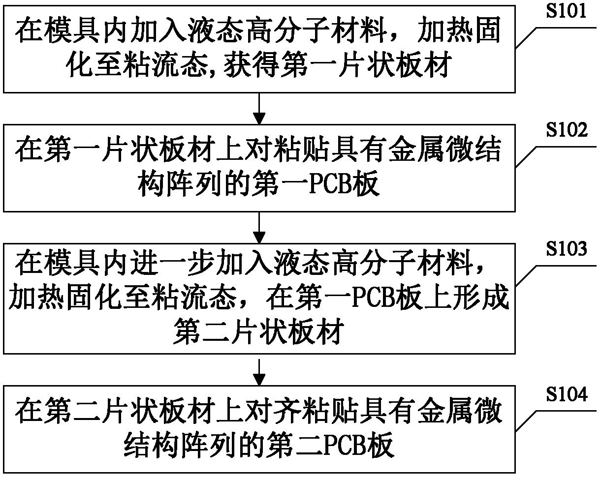
[0019] see figure 1 , is a flowchart of a method for preparing a metamaterial provided in Embodiment 1 of the present invention, and the method includes:
[0020] S101: adding a liquid polymer material into the mold, heating and curing to a viscous fluid state, and obtaining a first sheet-like plate.
[0021] Specifically, the liquid polymer material is a thermosetting resin, such as epoxy resin and silicone resin.
[0022] Among them, the volume of polymer material added to the mold is designed according to specific requirements, for example, 48-60 ml; the temperature of heating and curing is generally set according to the type of polymer material, for example, if the polymer material is silicone resin, then The curing temperature is 105-115°C.
[0023] S102: Paste the first PCB board with the metal microstructure array on the first sheet material.
[0024] Wherein, each metal microstructure in the metal microstructure array is an axisymmetric figure, for example, "I" and ...
Embodiment 2
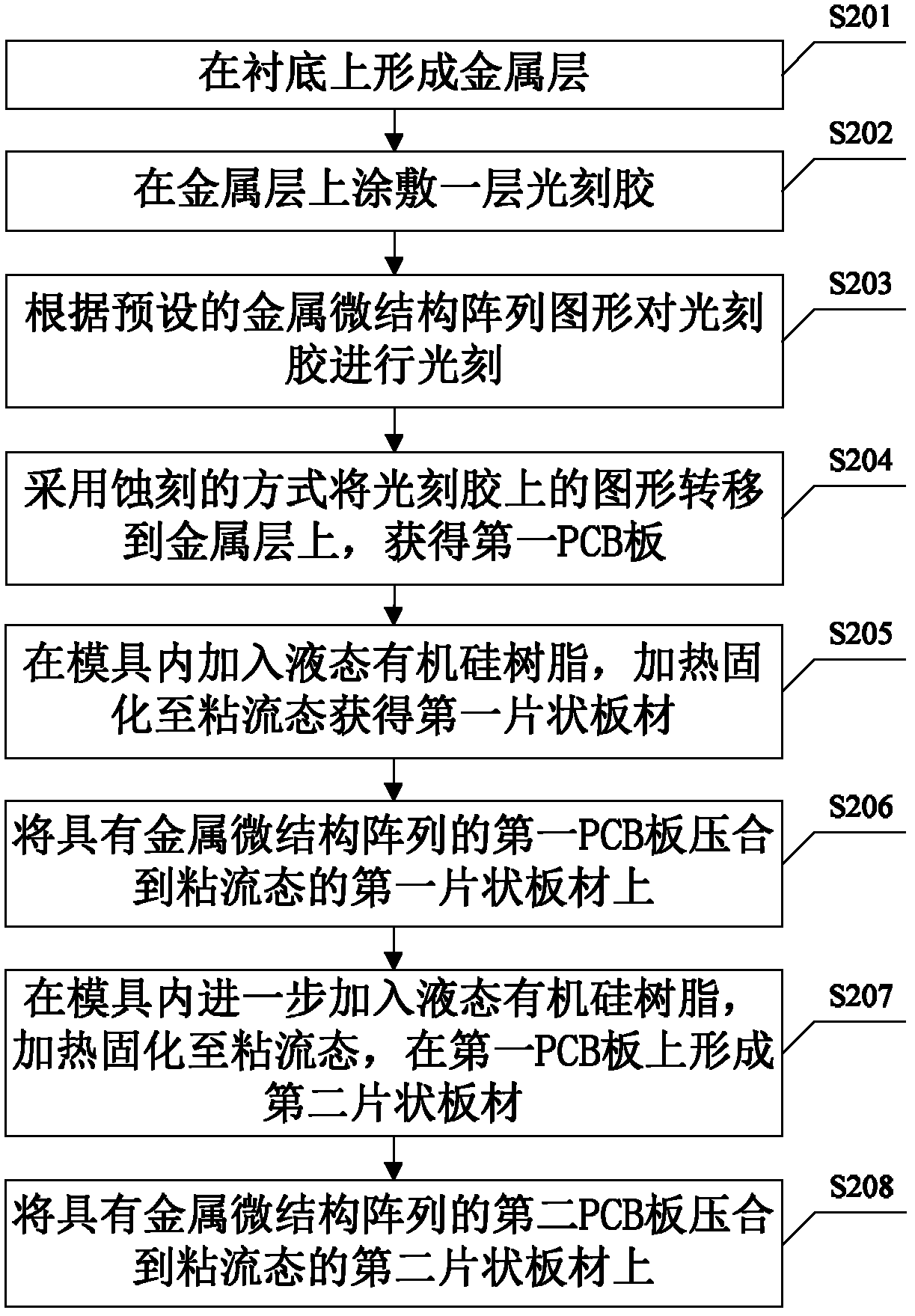
[0029] see figure 2 , is a flow chart of a method for preparing a metamaterial provided in Embodiment 2 of the present invention, and the preparation method includes:
[0030] S201: forming a metal layer on a substrate.
[0031] Specifically, a method of pasting a layer of metal with an adhesive on the substrate may be adopted; or a method of evaporating a metal layer on the substrate may be adopted.
[0032] S202: Coating a layer of photoresist on the metal layer.
[0033] S203: Perform photolithography on the photoresist according to the preset metal microstructure array pattern.
[0034] Wherein, each metal microstructure in the metal microstructure array is an axisymmetric figure, for example, "I" and its derivative figures, "big" and its derivative figures; it can also be a non-axisymmetric figure, for example, "卐" Glyphs and their derivative graphics, parallelograms.
[0035] S204: Transfer the pattern on the photoresist to the metal layer by etching to obtain a fir...
Embodiment 3
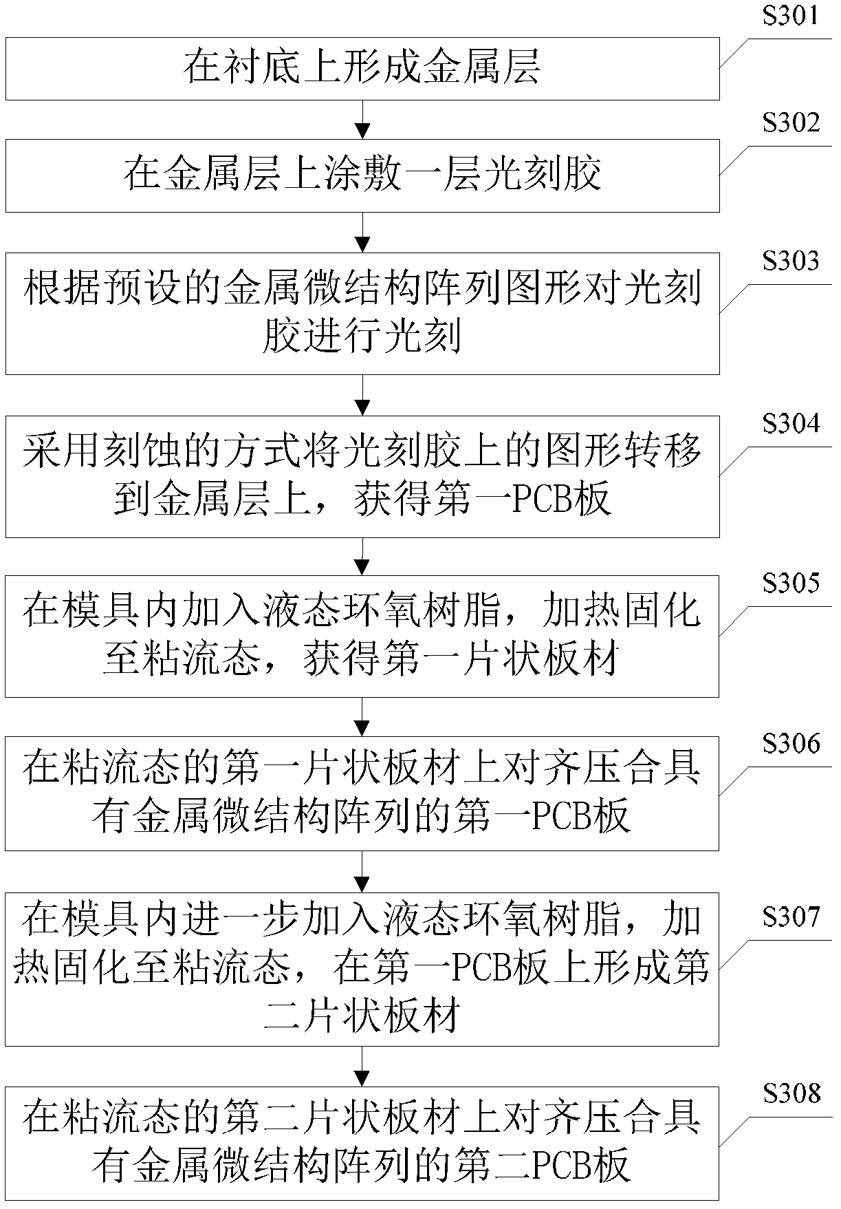
[0043] see image 3 , is a flow chart of a method for preparing a metamaterial provided in Embodiment 3 of the present invention, and the preparation method includes:
[0044] S301: forming a metal layer on a substrate.
[0045] Specifically, a method of pasting a layer of metal with an adhesive on the substrate may be adopted; or a method of evaporating a metal layer on the substrate may be adopted.
[0046] S302: Coating a layer of photoresist on the metal layer.
[0047] S303: Perform photolithography on the photoresist according to the preset metal microstructure array pattern.
[0048] Wherein, each metal microstructure in the metal microstructure array is an axisymmetric figure, for example, "I" and its derivative figures, "big" and its derivative figures; it can also be a non-axisymmetric figure, for example, "卐" Glyphs and their derivative graphics, parallelograms.
[0049] S304: Transfer the pattern on the photoresist to the metal layer by etching to obtain a firs...
PUM
 Abstract
Description
Claims
Application Information
 - R&D
- Intellectual Property
- Life Sciences
- Materials
- Tech Scout
- Unparalleled Data Quality
- Higher Quality Content
- 60% Fewer Hallucinations
Browse by: Latest US Patents, China's latest patents, Technical Efficacy Thesaurus, Application Domain, Technology Topic, Popular Technical Reports.
© 2025 PatSnap. All rights reserved.Legal|Privacy policy|Modern Slavery Act Transparency Statement|Sitemap|About US| Contact US: help@patsnap.com


